
Apparatus and Method for Using a Single Bank of eFuses to Successively Store Testing Data from Multiple Stages of Testing

a technology of electrical fuses and successive storage of testing data, applied in the field of data processing system and method, can solve the problems of large amount of efuses, waste of space, and inability to use in any subsequent stage of testing, and achieve the effect of avoiding large groups of data

Active Publication Date: 2008-05-01
META PLATFORMS INC
View PDF14 Cites 7 Cited by
  • Summary
  • Abstract
  • Description
  • Claims
  • Application Information

AI Technical Summary

Benefits of technology

[0013] The data programmed in the eFuses can be sensed and read as part of a scan chain. Thus, it can be easily determined what portions of the bank of eFuses have already been programmed by a previous stage of testing and where to start programming the next set of data into the bank of eFuses. As a result, the single bank of eFuses stores multiple sets of data from a plurality of test stages.
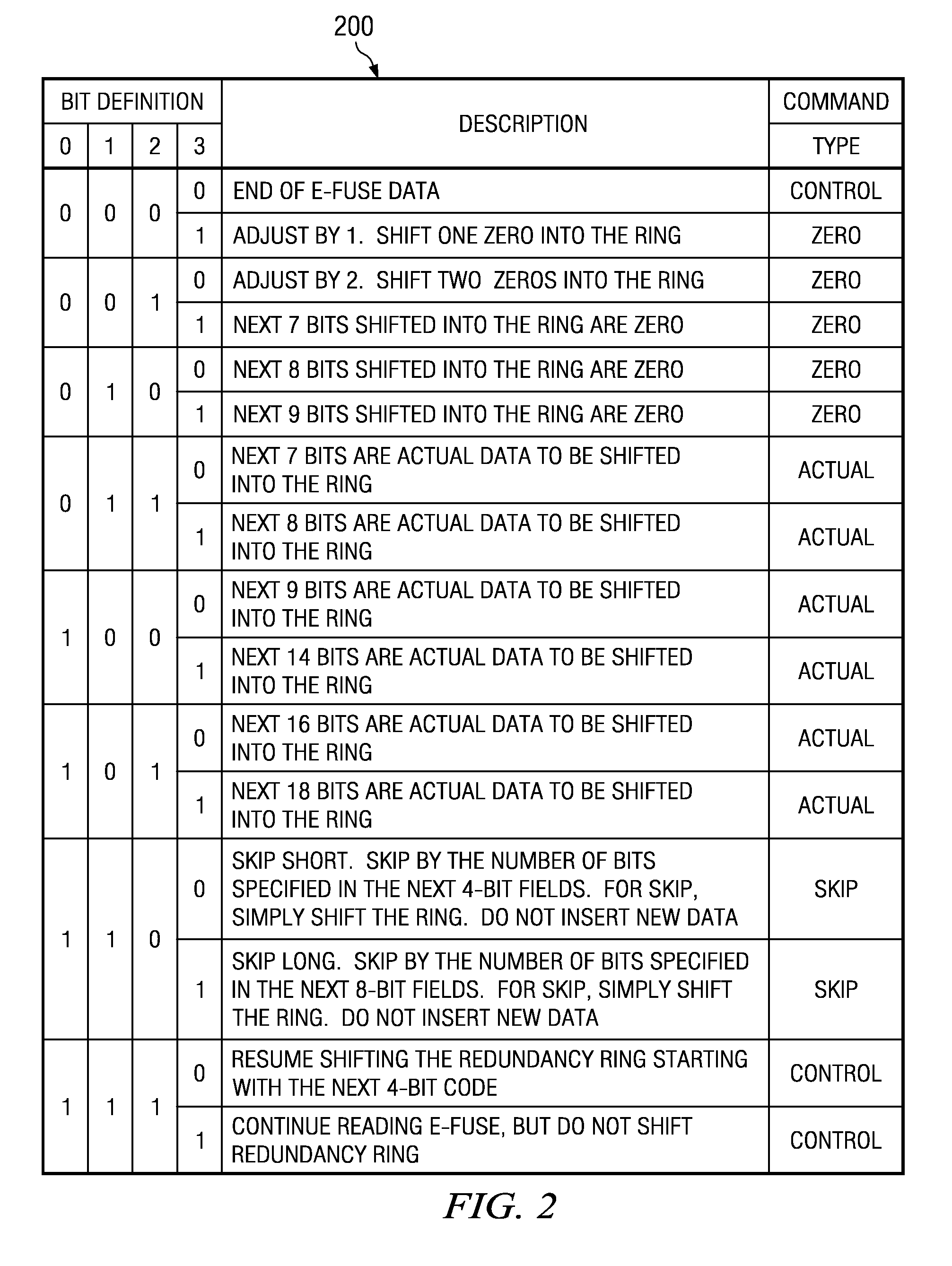
[0014] In addition, a data compression encoding technique is provided by the present invention to concisely encode a full redundancy ring. In particular, a skip command is provided for skipping to an appropriate portion of the bank of eFuses for writing and / or reading data to / from the bank of eFuses. The skip command does two things: (1) it allows the redundancy data to be concisely encoded via a long or short skip command followed by either 8 or 4 bits that specify how many bits to skip (up to 255 or up to 15 bits); and (2) it allows multiple passes when loading the actual redundancy ring because each pass can easily skip large groups of data, leaving the previous data in place for those components.

Problems solved by technology

On a large integrated circuit device or processor, there is a large amount of array redundancy data that can take up large amounts of eFuses.
Moreover, if there are any eFuses left over from one stage of testing, they cannot be used in any subsequent stage of testing.
Thus, the known mechanisms for storing and using array redundancy data from multiple stages of testing of an integrated circuit device result in excess area of the integrated circuit device or processor being dedicated to banks of eFuses and result in wasted space when eFuses are not able to be utilized from one stage of testing to the next.
This is undesirable in that the extra area and logic impact the function and cost of the overall integrated circuit device or processor.
Moreover, if the device is larger, then more power is needed to operate it.

Method used


Image

  • Apparatus and Method for Using a Single Bank of eFuses to Successively Store Testing Data from Multiple Stages of Testing
  • Apparatus and Method for Using a Single Bank of eFuses to Successively Store Testing Data from Multiple Stages of Testing
  • Apparatus and Method for Using a Single Bank of eFuses to Successively Store Testing Data from Multiple Stages of Testing

Examples


Embodiment Construction

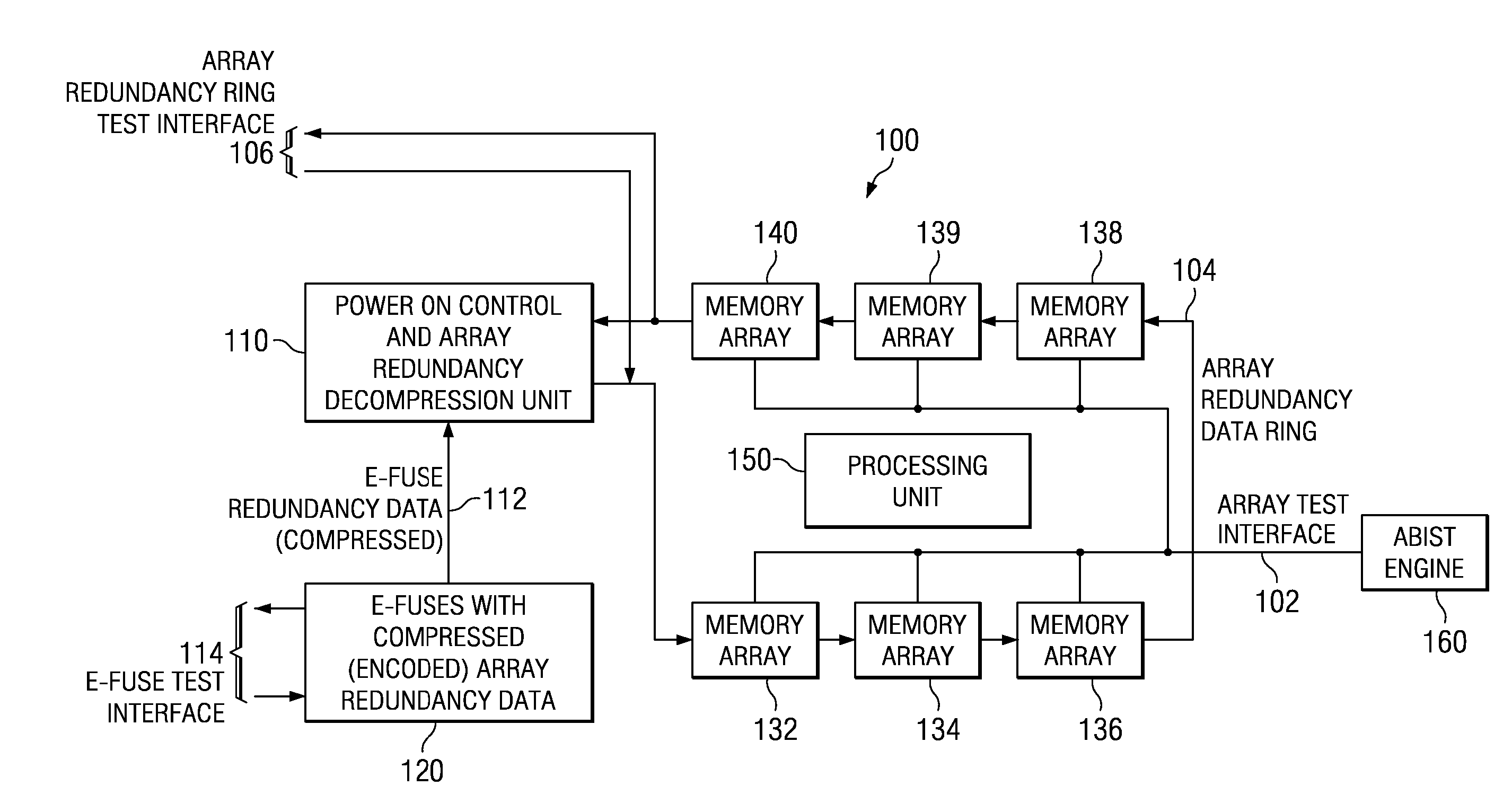
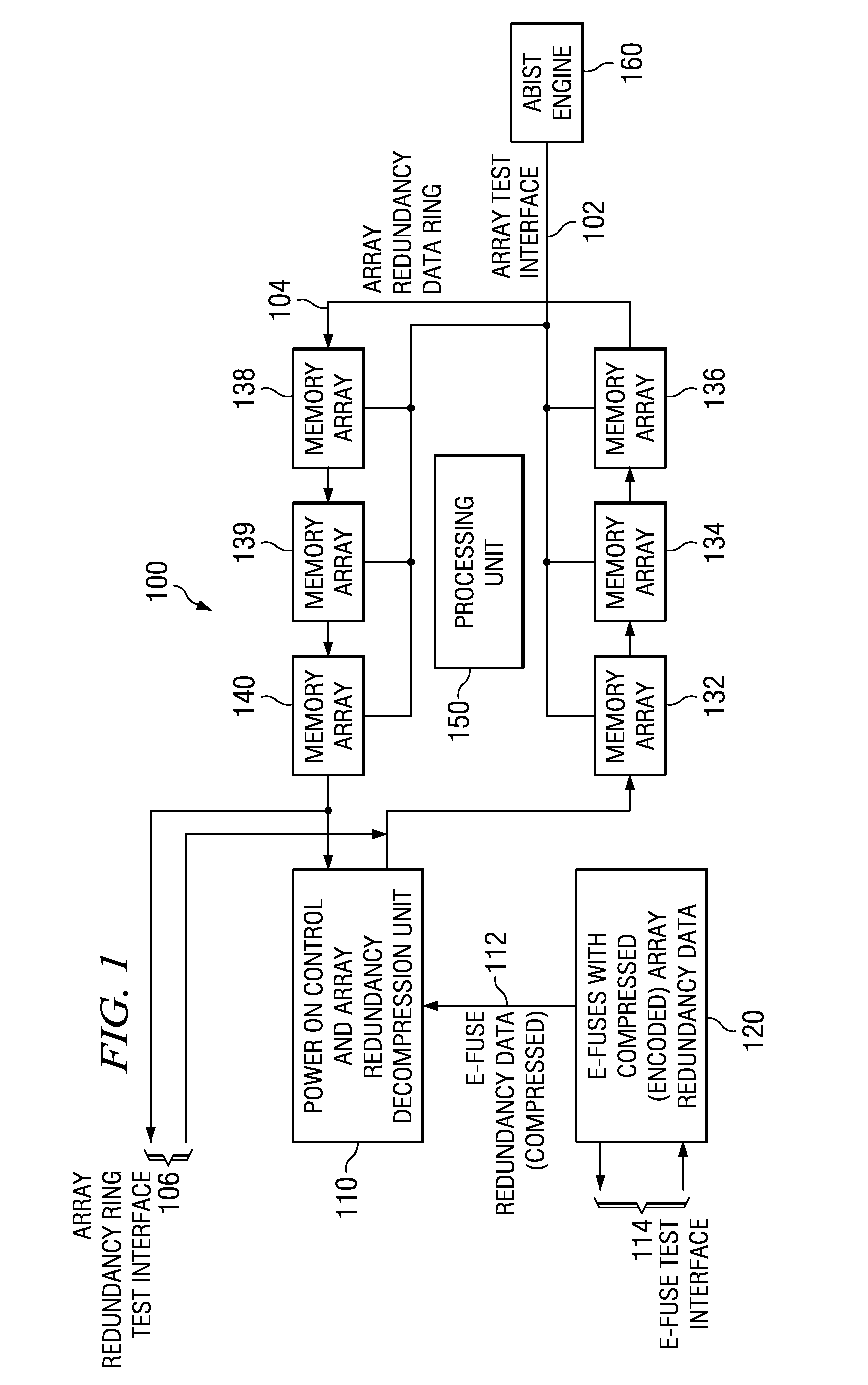
[0033] As mentioned above, the present invention is directed to an apparatus and method for using a single bank of storage devices, such as electric fuses (eFuses) or laser fuses, to successively store test data derived from multiple stages of testing. The present invention may be used with any apparatus in which an array of components is provided with one or more redundant components being provided in the array for substitution in the case of a failure of a component in the array. Such apparatus may take the form of an integrated circuit device, a microprocessor, or the like, for example. In the following exemplary embodiments, it will be assumed that the apparatus is a microprocessor having multiple memory arrays. However, it should be appreciated that these are only exemplary embodiments and the present invention is not limited to such embodiments.

[0034] Referring to FIG. 1, a diagram is provided that illustrates an exemplary block diagram of a modified array redundancy data rin...


PUM


Abstract

An apparatus and method for using a single bank of electric fuses (eFuses) to successively store test data derived from multiple stages of testing are provided. To encode and store array redundancy data from each subsequent test in the same bank of eFuses, a latch on a scan chain is used that holds the programming information for each eFuse. This latch allows for programming only a portion of eFuses during each stage of testing. Moreover, the data programmed in the eFuses can be sensed and read as part of a scan chain. Thus, it can be easily determined what portions of the bank of eFuses have already been programmed by a previous stage of testing and where to start programming the next set of data into the bank of eFuses. As a result, the single bank of eFuses stores multiple sets of data from a plurality of test stages.

Description

BACKGROUND OF THE INVENTION [0001] 1. Technical Field [0002] The present invention relates generally to an improved data processing system and method. More specifically, the present invention is directed to an apparatus and method for using a single bank of electrical fuses (eFuses) to successively store testing data from multiple stages of testing. [0003] 2. Description of Related Art [0004] Traditionally, the manufacturers of complex integrated circuits with arrays of components use multiple stages of testing to test the operation of the various components. For example, a manufacturer may first test the components of the integrated circuit at normal temperature and voltage in wafer form. The manufacturer may then run additional tests of the good components, i.e. those that pass the initial test, under stress. The manufacturer may then test the integrated circuit again when it is packaged. Other tests may also be included in the test regime to check the operation of the components ...

Claims


Application Information

Patent Timeline
Patent Type & Authority Applications(United States)
IPC IPC(8): G01R31/3187G06F11/26G06F11/27
CPCG11C29/44G11C29/72G11C2029/4402G11C29/802G11C2029/1208G11C29/789G11C29/00
Inventor RILEY, MACK WAYNE
Owner META PLATFORMS INC
Learn More