Light emitting diode assembly and method of fabrication

a technology of led arrays and diodes, applied in the direction of discharge tubes/lamp details, discharge tubes luminescnet screens, electric discharge lamps, etc., can solve the problems of reduced light output efficiency of leds, inefficient fabrication techniques, time-consuming and expensive, etc., to achieve excellent luminescence conversion and color mixing, efficient light extraction, and enhanced brightness and uniformity

Inactive Publication Date: 2008-05-15
INTEMATIX
View PDF3 Cites 32 Cited by
  • Summary
  • Abstract
  • Description
  • Claims
  • Application Information

AI Technical Summary

Benefits of technology

[0012]Disclosed in this patent are methods that provide integrated solutions to achieve efficient light extraction, excellent luminescence conversion and color mixing, directional illumination, and enhancement of brightness and uniformity for LED chips with phosphor coating and optical component mounting at LED wafer level. The optical component may be a lens array with a phosphor coating or embedded phosphor particles. The process of applying the lens array and phosphors may be by lithographic method directly to LED wafers. The structures and processes disclosed in this patent can significantly improve production consistency and manufacturing cost efficiency. The application of an optical lens arrays applied can significantly improve light extraction and light luminescent conversion performance, and significantly improve the manufacturing quality consistency.

Problems solved by technology

In addition absorption within the LED material and Fresnel reflection loss at the interface reduce the light output efficiency of the LED.
A problem with mounting such lenses is that due to the size of the LED chip, which is typically a few microns, the tolerances for aligning the lens with the chip are very precise and the process can become expensive.
Such a fabrication technique is inefficient, time consuming and expensive.
However, individually packaging phosphor materials along with lenses at discrete chip level is still a time-consuming process.

Method used


Image

  • Light emitting diode assembly and method of fabrication
  • Light emitting diode assembly and method of fabrication
  • Light emitting diode assembly and method of fabrication

Examples


Embodiment Construction

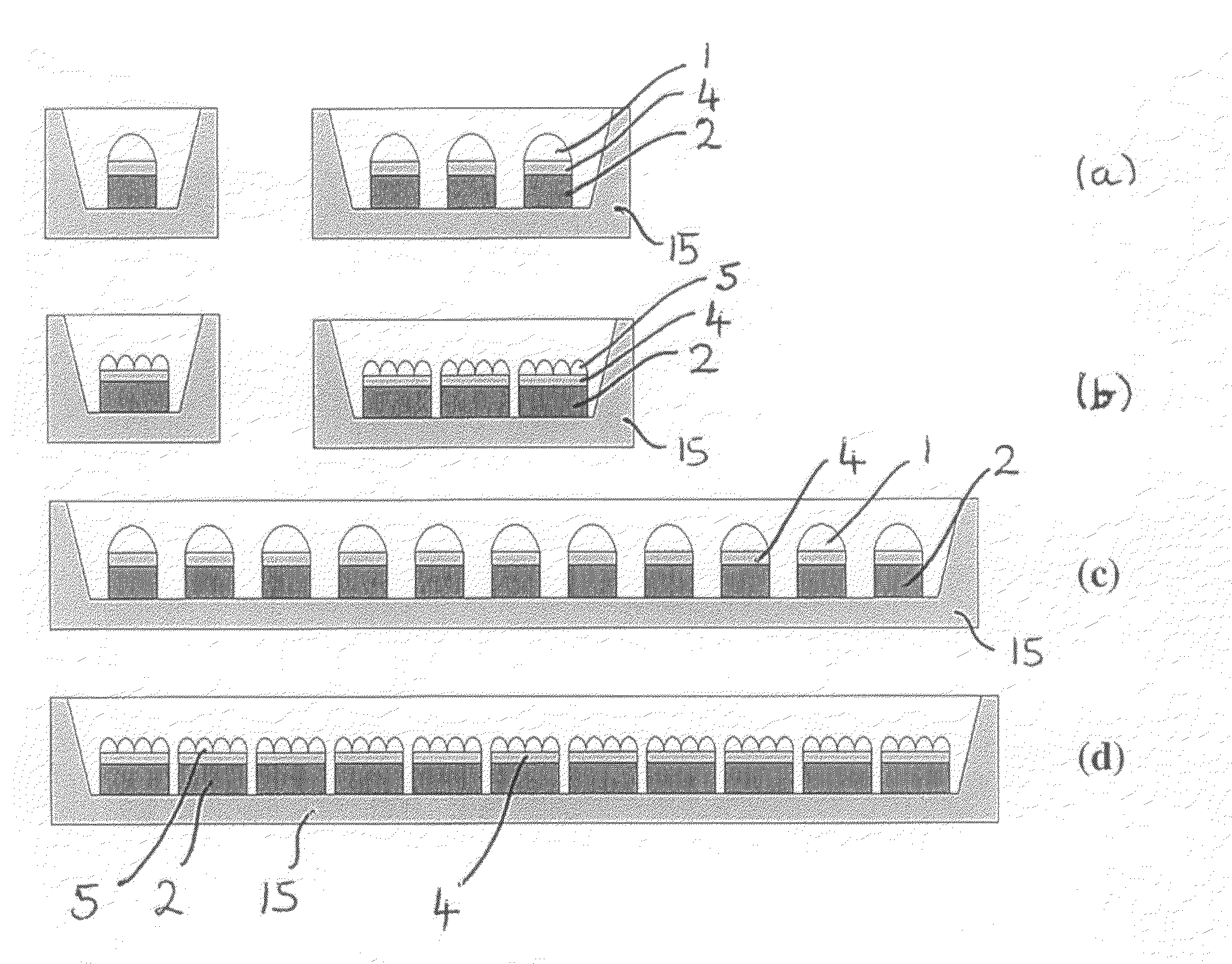
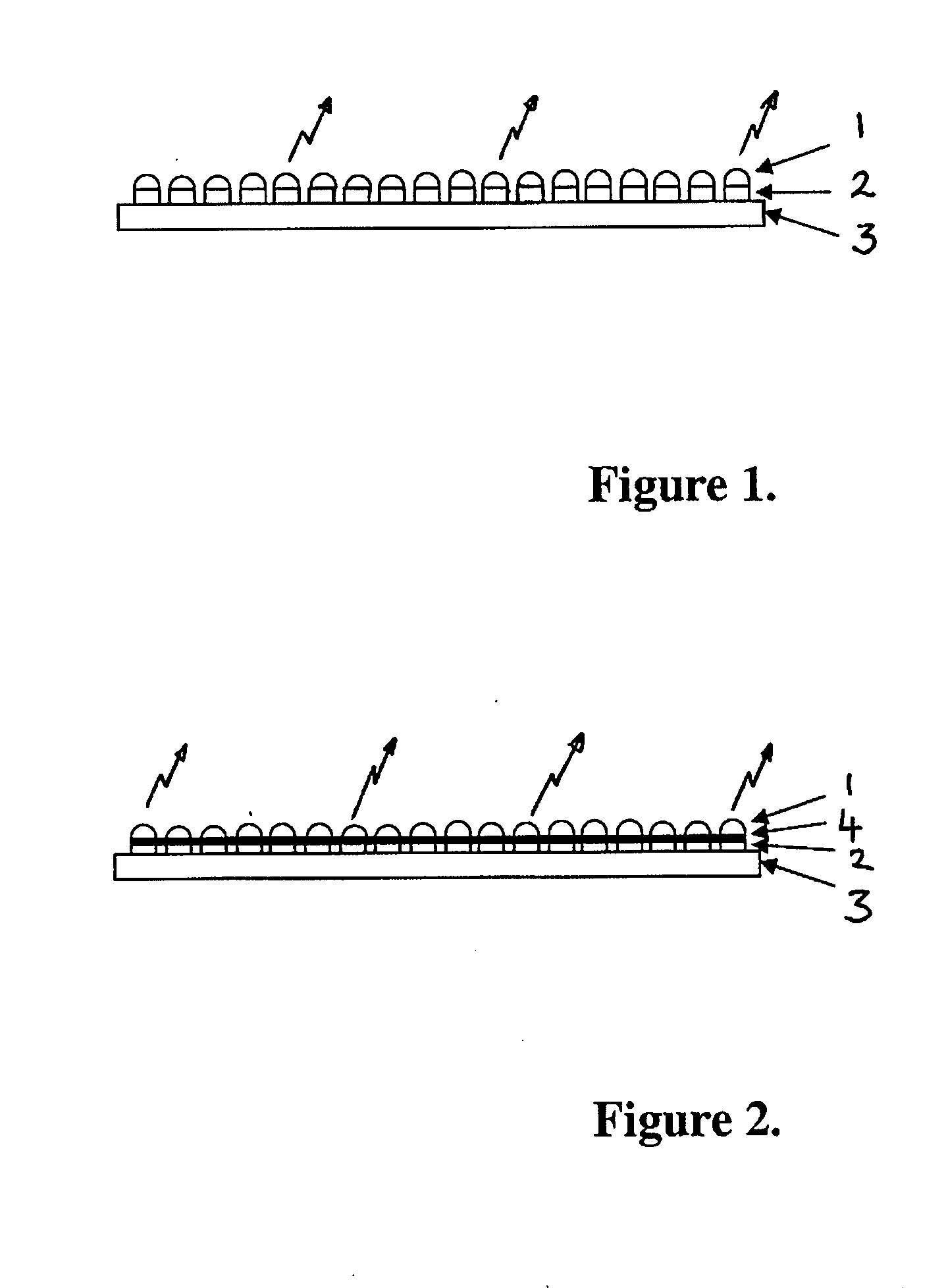
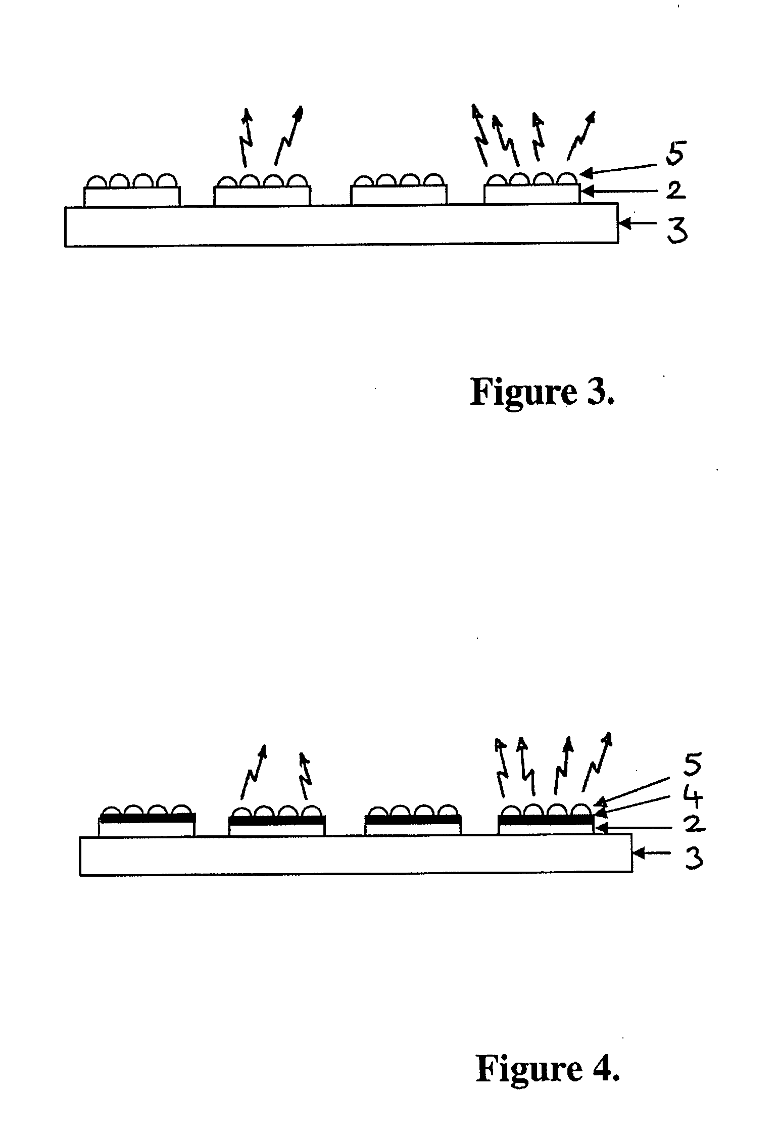
[0029]Disclosed herein are methods of making a device comprising a LED chip and associated lens with or without phosphor material for color mixing and luminescence conversion in volume at wafer level. A lens array may be positioned adjacent to an array of LED dies processed on a substrate referred to as an LED wafer, wherein there is a correspondence between the individual lenses of the lens array and the individual LED dies on the wafer. The lens array may be fabricated using lithographic techniques including molding, casting, and imprinting. The array of LED dies on the wafer may exclusively be GaN (gallium nitride) based LEDs. In the context of this patent application light emitting diode (LED) is to be construed as meaning any solid-state light source and can include for example laser diodes.

LED Assemblies and Arrays

[0030]In one embodiment of the invention, the individual elements (lenses) of the lens array may have the dimensions which substantially match the size of the LED di...


PUM


Abstract

An LED assembly comprises an LED and a lens disposed adjacent to a light emitting surface of the LED. The area of cross-section of the lens projected onto the light emitting surface of the LED is substantially equal to or less than the area of the LED's light emitting surface. The light emitting device can comprise an array of LEDs and an array of lenses, in which at least one lens is associated with each member of the LED array and wherein the area of a cross-section of each lens projected onto the light emitting surface of its associated LED is substantially equal to or less than the area of the LED's light emitting surface.

Description

CROSS REFERENCE TO RELATED APPLICATIONS[0001]This application claims priority to U.S. Provisional Application Ser. No. 60 / 858,211 filed Nov. 9, 2006 entitled “Light Emitting Diode Lens Assembly and Arrays thereof with Phosphor Enhancement” which is incorporated by reference herein in its entirety.BACKGROUND OF THE INVENTION[0002]1. Field of the Invention[0003]The present invention relates to light emitting devices comprising light emitting diode (LED) assemblies and LED array assemblies and methods of fabrication thereof. More especially, the invention concerns LED lens assemblies and LED array lens assemblies. Moreover, although not exclusively, the invention concerns LED assemblies with phosphor enhancement.[0004]2. Description of the Related Art[0005]Achieving the brightness expected from today's light emitting diodes (LEDs) requires efficiently extracting the light generated by the LED chip / die. LED chips typically have either an edge-emitting or surface-emitting structure. Tota...

Claims


Application Information

Patent Timeline
Patent Type & Authority Applications(United States)
IPC IPC(8): H01L33/00H01L21/00H01L33/50H01L33/54
CPCH01L25/0753H01L33/54H01L33/50H01L2924/0002H01L2924/00
Inventor LI, YI-QUNDONG, YISHAN, WEI
Owner INTEMATIX
Why Eureka
Try Eureka