Tft-lcd array substrate and manufacturing method thereof

a technology of thin film transistors and array substrates, applied in the field of thin film transistor liquid crystal display array substrates, can solve the problems of display quality degradation, defective such as mura, display quality degrade, etc., and achieve the effect of reducing the influence of flicker and mura on image quality

Inactive Publication Date: 2008-05-15
BEIJING BOE OPTOELECTRONCIS TECH CO LTD
View PDF1 Cites 29 Cited by
  • Summary
  • Abstract
  • Description
  • Claims
  • Application Information

AI Technical Summary

Benefits of technology

[0011]In view of the above problems, according to an aspect of the present invention, there is provided a TFT-LCD array substrate with a self-compensating parasitic capacitor structure and the manufacturing method thereof. When the process conditions are unstable and the overlapping area of the parasitic capacitor changes, a self-compensating function can be realized by the change of the compensating parasitic capacitor, so that the total capacitance of the parasitic capacitor Cgs of each sub-pixel is kept constant, the shift of ΔVp among the sub-pixels is uniform, and the influence of the phenomena of flicker and Mura on the image quality will decrease.
[0020]As compared with the conventional array substrate, by providing a self-compensating capacitor structure comprising the compensating parasitic capacitor Cgs2 in the present invention, when the process conditions are unstable and the shift of the source electrode with respect to the gate electrode is induced, the normal parasitic capacitor Cgs1 and the compensating parasitic capacitor Cgs2 can compensate with each other, so that the total capacitance of the parasitic capacitor Cgs of the sub-pixel structure can remain constant. Therefore, the performance degradation due to the non-uniform parasitic capacitor Cgs among the sub-pixels can be suppressed, the image quality of the product can be improved, and the yield of the product can be increased.

Problems solved by technology

However, the gate electrode and the source electrode of the TFT are partially overlapped, which results in the parasitic capacitor Cgs.
If the ΔVp′ is not equal to 0, the gray scale of the adjacent or nearby sub-pixels will not be uniform, so that display quality degrades and the defective such as Mura can appear.
However, when the instability in process condition induces the shift of the source electrode with respect to the gate electrode, the overlapping area between the source electrode and the gate electrode changes among sub-pixels, which results in Cgs different in magnitude, and the levels of gray scale in the adjacent or nearby sub-pixels are not uniform.
In this case, the brightness in some regions is too high (white) while in some other regions is insufficient (black), thus the phenomenon of non-uniform gray scale of the image such as Mura appears.
However, when the process conditions are unstable, which is generally inevitable during the manufacturing, there are two cases in which the source electrode 8 will shift with respect to the gate electrode 1.

Method used


Image

  • Tft-lcd array substrate and manufacturing method thereof
  • Tft-lcd array substrate and manufacturing method thereof
  • Tft-lcd array substrate and manufacturing method thereof

Examples


first embodiment

The First Embodiment

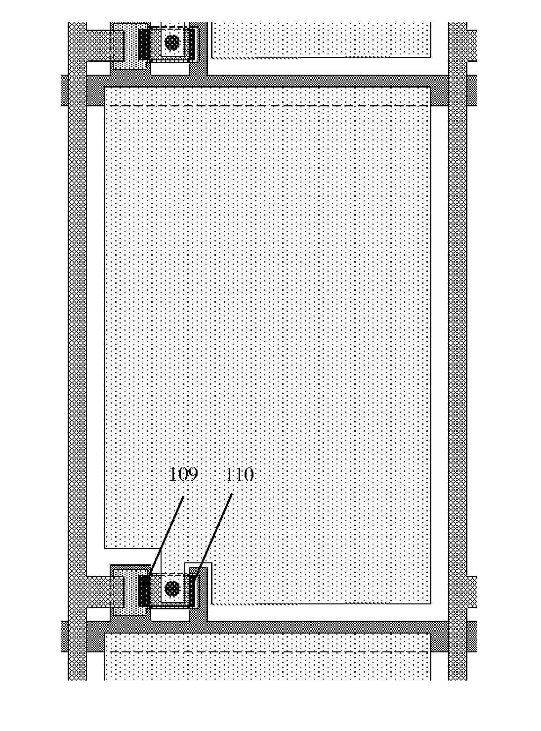
[0055]FIG. 5A is a schematic view showing the sub-pixel structure of the TFT-LCD array substrate with a self-compensating parasitic capacitor structure according to the first embodiment of the present invention. As shown in FIG. 5A, in addition to an overlapping region 109 of a gate electrode 101 and a source electrode 108 which form the normal parasitic capacitor Cgs1, an overlapping region 110 between a compensating source electrode 115 and the compensating gate electrode 117 is produced to form a compensating parasitic capacitor Cgs2, i.e., the self-compensating parasitic capacitor structure of the first embodiment. In the first embodiment, the parasitic capacitor Cgs1 and the compensating parasitic capacitor Cgs2 are formed at the positions of the TFT in the horizontal direction, as shown in FIG. 5A. The parasitic capacitor Cgs1 and the compensating parasitic capacitor Cgs2 are connected in parallel with each other, and the sum of these capacitors constitutes...

second embodiment

The Second Embodiment

[0060]FIG. 6A is a schematic view showing the sub-pixel structure of the TFT-LCD array substrate with a self-compensating parasitic capacitor structure according to the second embodiment of the present invention. FIG. 6B is an enlarged view showing the TFT device in FIG. 6A.

[0061]As shown in FIGS. 6A and 6B, the sub-pixel structure of the second embodiment is substantially similar to that in the first embodiment, and the difference lies in the overlapping structure realizing the compensating parasitic capacitor. In both the first and second embodiments, the compensating parasitic capacitor Cgs2 is realized by superposing the compensating source electrode 117 over the compensating gate electrode 115. However, in the compensating parasitic capacitor in the first embodiment, the compensating gate electrode 115 in the overlapping region 110 has a larger width, so that the width of the overlapping region 110 is determined by the width of the compensating source elect...

third embodiment

The Third Embodiment

[0062]FIG. 7A is a schematic view showing the sub-pixel structure of the TFT-LCD array substrate with a self-compensating parasitic capacitor structure according to the third embodiment of the present invention; FIG. 7B is an enlarged view showing the TFT device in FIG. 7A; and FIG. 7C is a cross-sectional view taken along the line C-C in FIG. 7B.

[0063]As shown in FIGS. 7A˜7C, the TFT and the compensating parasitic capacitor Cgs2 according to the third embodiment are disposed on two sides of the pixel electrode near the data lines, respectively. The TFT in the third embodiment is the same as that in the first embodiment, the parasitic capacitor structure is similar to that in the first embodiment, and the difference lies in that: in the third embodiment, the gate electrode 101 and the compensating gate electrode 115 are separated apart far away from each other in the extending direction of the gate line, the active layer 103 and the compensating active layer 116 ...


PUM

PropertyMeasurementUnit
widthaaaaaaaaaa
lengthaaaaaaaaaa
widthaaaaaaaaaa

Abstract

A TFT-LCD array substrate and a method for manufacturing the same. The TFT-LCD array substrate includes a substrate, on which at least one gate line and at least one data line are formed and cross with each other to define sub-pixel regions, one of the sub-pixel regions includes a thin film transistor (TFT) and a pixel electrode, and the TFT is electrically connected to the pixel electrode. The TFT-LCD array substrate further includes a compensating parasitic capacitor structure comprising a first electrode electrically connected to the gate line and a second electrode electrically connected to the pixel electrode.

Description

FIELD OF THE INVENTION[0001]The present invention relates to a thin film transistor liquid crystal display (TFT-LCD) array substrate and a manufacturing method thereof, and more particularly, to a TFT-LCD array substrate with a self-compensating parasitic capacitor structure and a manufacturing method thereof.BACKGROUND OF THE INVENTION[0002]In a TFT-LCD, the display of images is realized by changing the transmittance of the pixel points arrayed on a panel. A TFT-LCD includes many pixels, each of which in turn is composed of, for example, three sub-pixels (for example, R, G, and B sub-pixels), and can display, for example, 256 or more levels in gray scale. To display a desired image, it is necessary to control the gray scale of each sub-pixel. Each sub-pixel is controlled by a thin film transistor (TFT) as a switching element. A TFT-LCD includes an array substrate, a color film substrate, and a liquid crystal layer interposed between the substrates.[0003]On the array substrate, a pl...

Claims


Application Information

Patent Timeline
Patent Type & Authority Applications(United States)
IPC IPC(8): G02F1/133G02F1/1368H01L21/77
CPCG02F2001/13606H01L27/124H01L27/1255G02F1/13606G02F1/136
Inventor WU, HONGJIANGWANG, WEILONG, CHUNPINGLEE, CHANG HEE
Owner BEIJING BOE OPTOELECTRONCIS TECH CO LTD
Why Eureka
Try Eureka