Plasma-enhanced deposition of metal carbide films

a metal carbide film and plasma technology, applied in the field of metal carbide films, can solve the problems of insufficient film coverage in shaded areas of complex substrate contours, difficult to obtain traditional methods, and high relative temperature of substrates,

Active Publication Date: 2008-05-15
ASM IP HLDG BV
View PDF99 Cites 63 Cited by
  • Summary
  • Abstract
  • Description
  • Claims
  • Application Information

AI Technical Summary

Benefits of technology

[0015]According to one aspect of the invention, methods for growing a metal carbide film over a substrate are provided. The methods generally comprise contacting a substrate in a reaction space with a first reactant that includes a metal source chemical and a second reactant that includes one or more plasma-excited species of a carbon-containing compound, thereby forming the metal carbide film over the substrate. The substrate is also contacted with a third reactant, which is a reducing agent. In some embodiments, the reducing agent contacts the substrate after contacting the substrate with the first reactant and before contacting the substrate with the second reactant. In some other embodiments, the reducing agent contacts the substrate after contacting the substrate with the second reactant and before contacting the substrate with the first reactant an additional time.
[0016]According to some embodiments of the invention, atomic layer deposition (ALD) processes for growing a metal carbide film over a substrate comprise alternately and sequentially contacting a substrate in a reaction space with vapor phase pulses of a metal compound that forms no more than about one monolayer of a metal-containing film on an exposed surface of the substrate, and one or more plasma-excited species of a carbon-containing compound. In addition, the substrate is exposed to one or more vapor phase pulses of a reducing agent between pulses of the metal compound and the carbon-containing compound. The reducing agent may be, for example, a plasma-excited species of H2.
[0017]According to other embodiments of the invention, chemical vapor deposition (CVD) processes for growing a metal carbide film over a substrate comprise simultaneously contacting the substrate with a metal compound and one or more plasma-excited species of a carbon-containing compound to form a metal carbide film. The substrate is also contacted with a reducing agent. The reducing agent contacts the substrate after, e.g., contacting the substrate with the metal compound.

Problems solved by technology

Design rules are setting the feature sizes to ≦0.2 μm, making complete film coverage on deep bottoms and vias difficult to obtain by traditional methods.
A problem with the disclosed process is that the substrate temperature is rather high relative to thermal budgets for state-of-the-art semiconductor fabrication, particularly in metallization stages.
Line-of-sight deposition, however, means that complex substrate contours will have insufficient film coverage in shaded areas.

Method used


Image

  • Plasma-enhanced deposition of metal carbide films
  • Plasma-enhanced deposition of metal carbide films

Examples


example

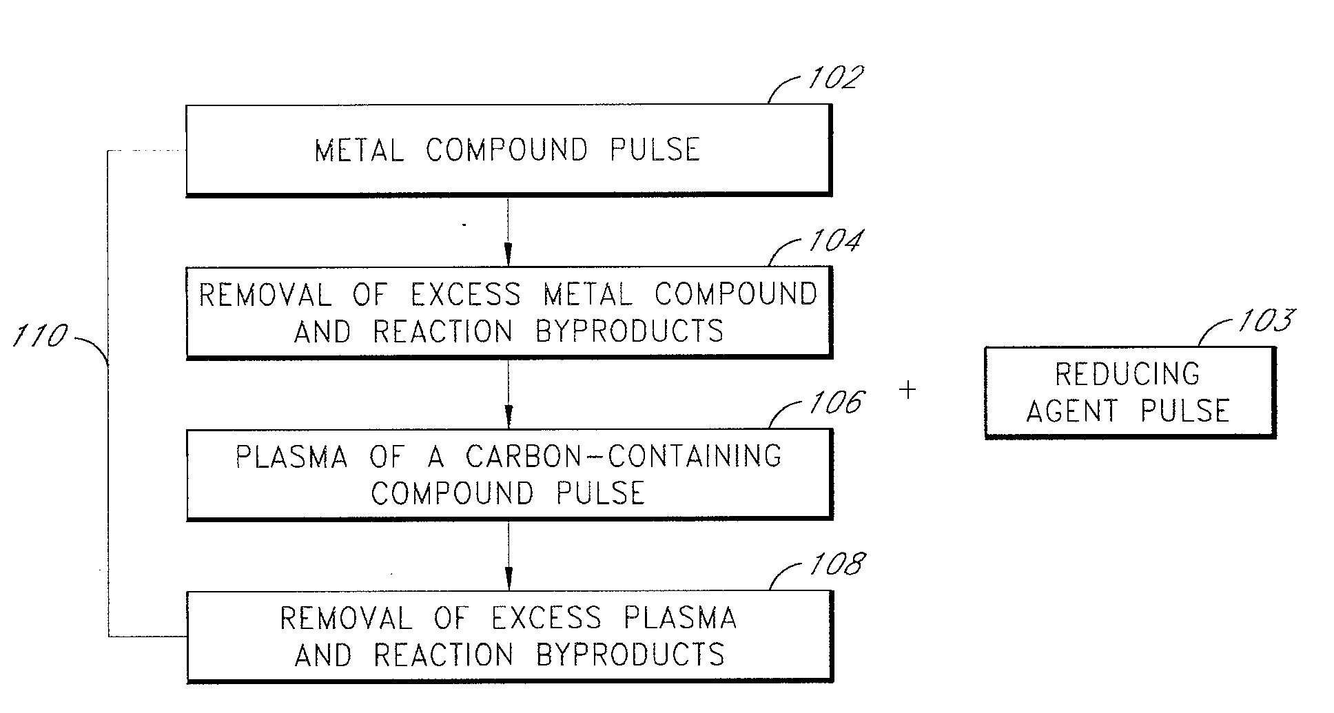
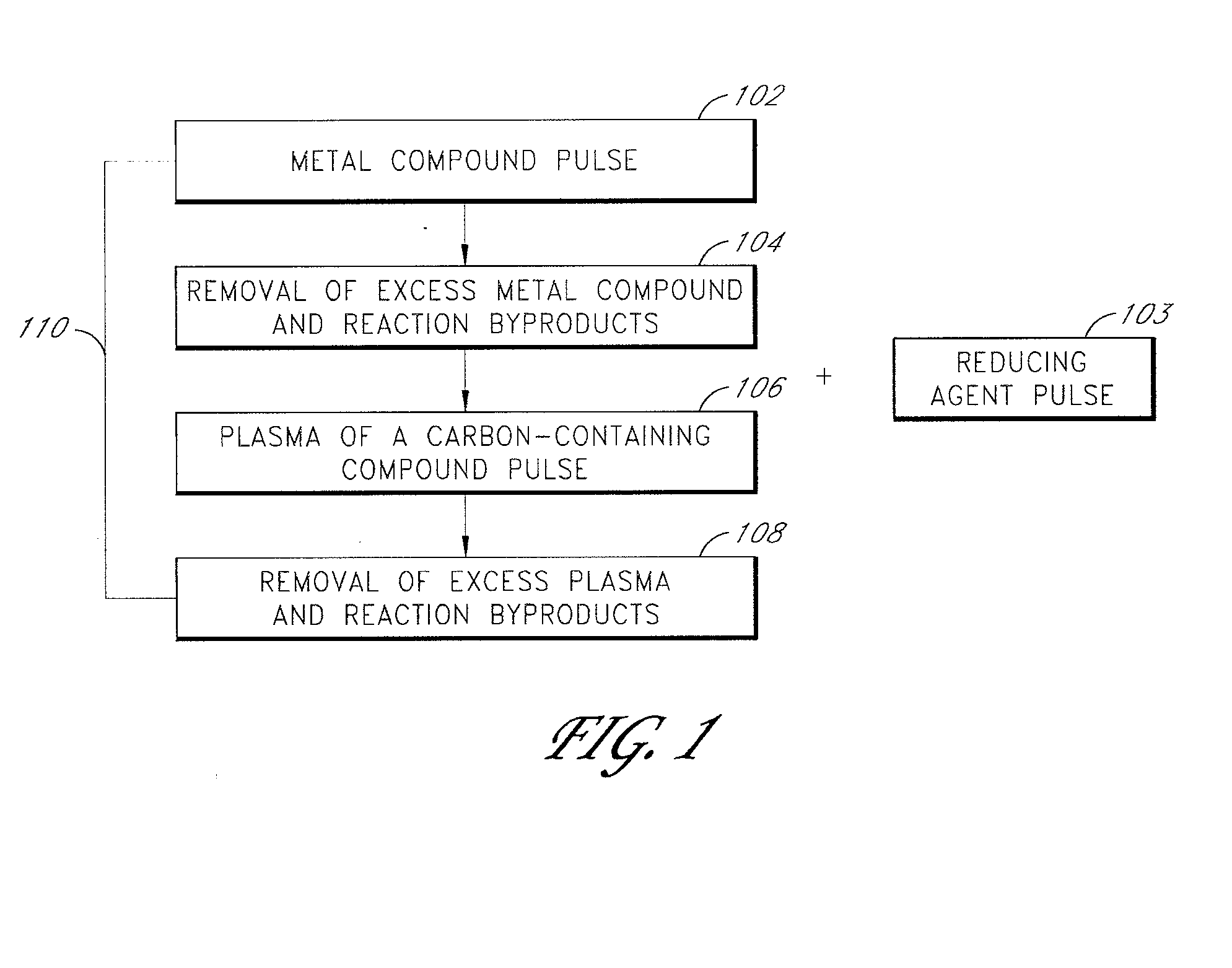
[0076]A tantalum carbide film was deposited on a silicon dioxide (SiO2) substrate in an ALD-type process. The sequence of steps included alternately and sequentially pulsing a metal compound (TaF5), plasma-excited species of a carbon-containing compound (CH4) and a purge gas (Ar) into a reaction space comprising the substrate. The substrate was supported on a susceptor in a showerhead-type PEALD reactor manufactured by ASM Genitech, Inc. Deposition was conducted at a substrate temperature of about 350° C. The TaF5 source gas was maintained at a temperature of about 95° C. Methane (CH4) was introduced into the reactor at a flow rate between about 100-500 sccm. The flow rate of the argon (Ar) purge gas was held at approximately 650 sccm. CH4 plasma (CH4*) was generated by supplying power (about 200-700 W) to a showerhead disposed over the substrate. The sequence of gas pulses and pulsing times (milliseconds, “ms”) were as follows:

[0077](1) TaF5 pulse (900 ms);

[0078](2) Ar purge (3000 ...


PUM

PropertyMeasurementUnit
feature sizesaaaaaaaaaa
thicknessaaaaaaaaaa
thicknessaaaaaaaaaa

Abstract

Methods of forming a metal carbide film are provided. In some embodiments, methods for forming a metal carbide film in an atomic layer deposition (ALD) type process comprise alternately and sequentially contacting a substrate in a reaction space with vapor phase pulses of a metal compound and one or more plasma-excited species of a carbon-containing compound. In other embodiments, methods of forming a metal carbide film in a chemical vapor deposition (CVD) type process comprise simultaneously contacting a substrate in a reaction space with a metal compound and one or more plasma-excited species of a carbon-containing compound. The substrate is further exposed to a reducing agent. The reducing agent removes impurities, including halogen atoms and/or oxygen atoms

Description

REFERENCE TO RELATED APPLICATIONS[0001]The present Application claims the priority benefit under 35 U.S.C. §119(e) of U.S. Provisional Patent Application No. 60 / 854,609, filed Oct. 25, 2006, entitled PLASMA-ENHANCED DEPOSITION OF METAL CARBIDE FILMS.[0002]In addition, the present application is related to and incorporates the following by reference in their entireties: U.S. patent application Ser. No. 10 / 246,131 to Elers et al., filed Sep. 17, 2002, now U.S. Pat. No. 6,800,552; and U.S. patent application Ser. No. 10 / 394,309 to Saanila et al., filed Mar. 20, 2003, now U.S. Pat. No. 6,794,287.BACKGROUND OF THE INVENTION[0003]1. Field of the Invention[0004]The present invention relates to metal carbide films. In particular, the invention concerns methods of growing metal carbide films by vapor deposition processes.[0005]2. Description of the Related Art[0006]The integration level of components in integrated circuits is increasing rapidly, which demands a decrease of the size of integr...

Claims


Application Information

Patent Timeline
Patent Type & Authority Applications(United States)
IPC IPC(8): C23C16/00H05H1/24
CPCC23C16/32C23C16/515C23C16/45542C23C16/45527
Inventor ELERS, KAI-ERIKWILK, GLENMARCUS, STEVEN
Owner ASM IP HLDG BV
Why Eureka
Try Eureka