Scanning Electron Microscope Having Time Constant Measurement Capability

a scanning electron microscope and measurement capability technology, applied in the field of electron microscopes, can solve the problems of distortion of images obtained by scanning electron microscopes, difficult to measure true dimensions and shapes after processing, and error in dimension measurement, etc., and achieve accurate and stable images.

Active Publication Date: 2008-05-22
HITACHI HIGH-TECH CORP
View PDF4 Cites 14 Cited by
  • Summary
  • Abstract
  • Description
  • Claims
  • Application Information

AI Technical Summary

Benefits of technology

[0026]According to the present invention, an optimum scanning order (most resistant to the influence of charging produced by el...

Problems solved by technology

The charged specimen not only changes the amount of secondary electrons that attempt to escape from the surface of the specimen but also bends the trajectory of the primary electron beam, resulting in distortion of images obtained by a scanning electron microscope.
As a result, it is difficult to measure true dimensions and shapes after processing.
For example, in the case of an ArF resist, it cannot ...

Method used


Image

  • Scanning Electron Microscope Having Time Constant Measurement Capability
  • Scanning Electron Microscope Having Time Constant Measurement Capability
  • Scanning Electron Microscope Having Time Constant Measurement Capability

Examples


Embodiment Construction

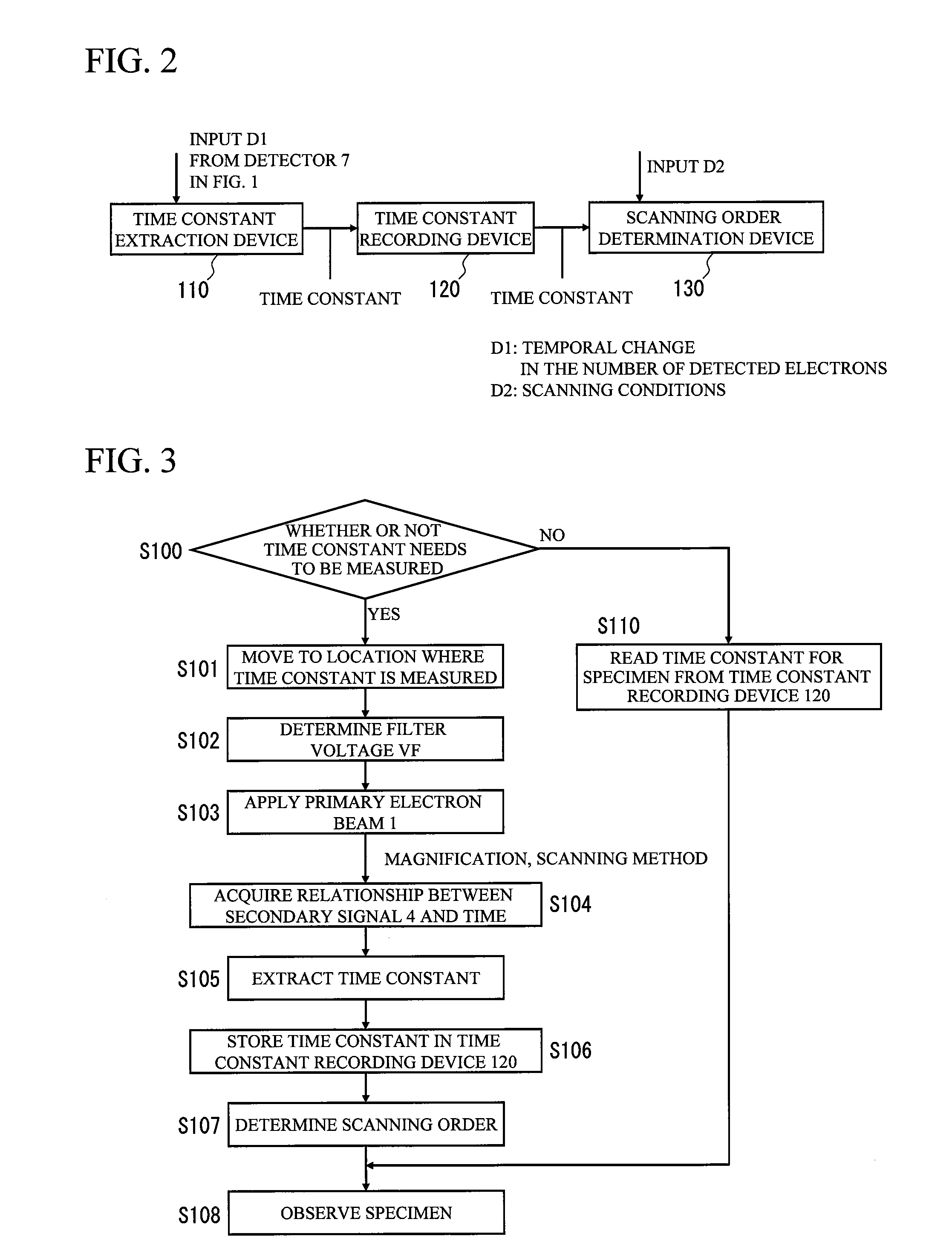
[0035]An embodiment according to the present invention will be described below in detail with reference to the accompanying drawings. The embodiment according to the present invention is only an example to implement the present invention, and the present invention is not limited thereto.

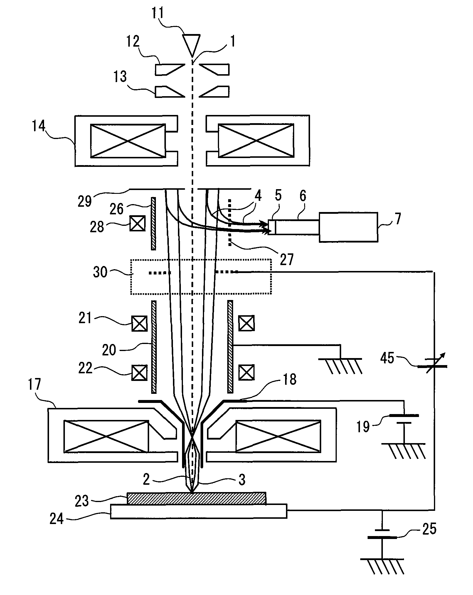
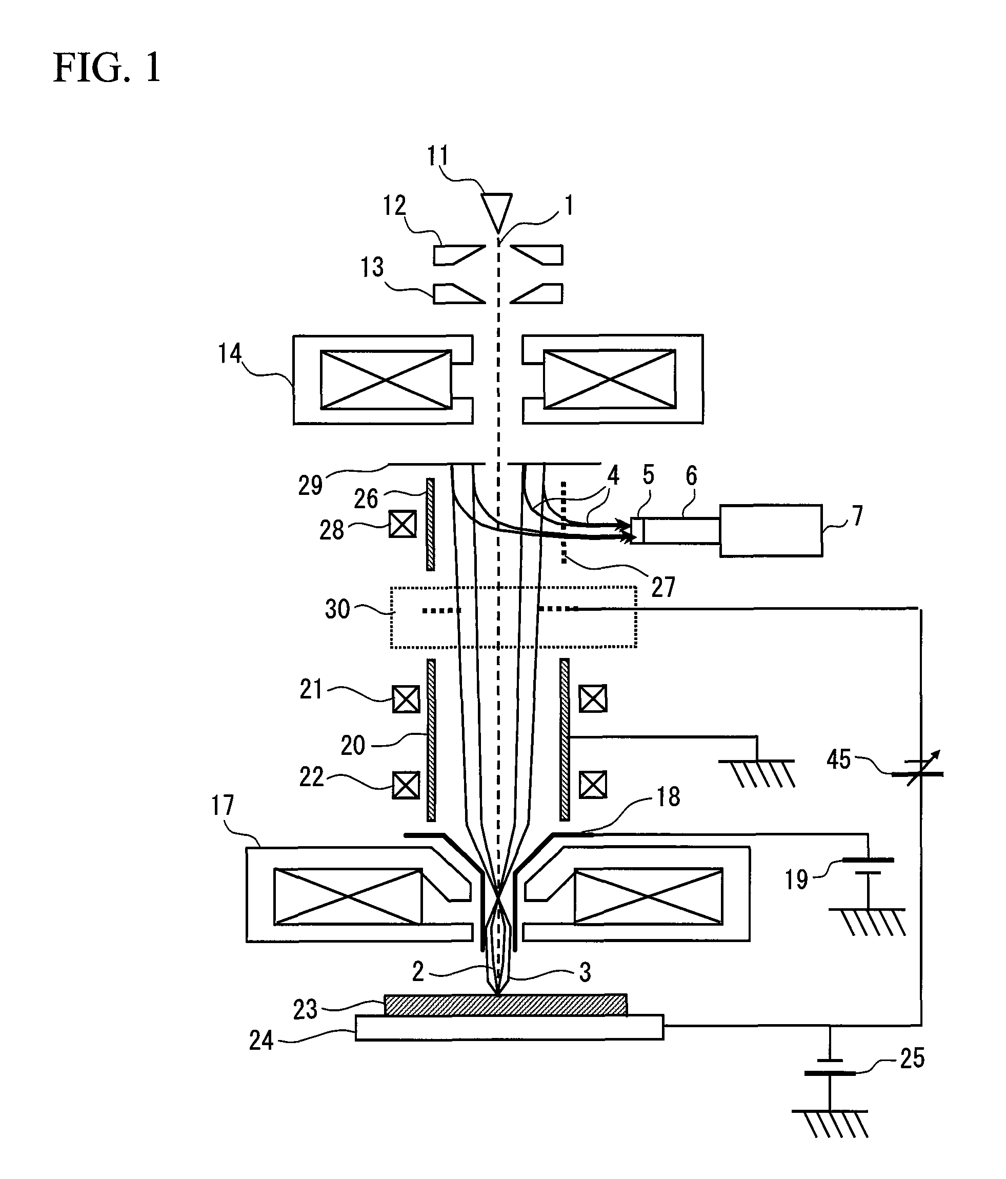
[0036]FIG. 1 shows a schematic configuration of a SEM (Scanning Electron Microscope) used in the embodiment of the present invention. An extracting voltage 13 is applied between a field emission electrode 11 and an extracting electrode 12 to generate a primary electron beam 1. The primary electron beam 1 undergoes scanning deflection through a condenser lens 14, an upper scanning deflector 21, and a lower scanning deflector 22. The magnitude of deflection produced in the upper scanning deflector 21 and the lower scanning deflector 22 is adjusted in such a way that a specimen 23 is scanned in a two dimensional manner using the center of an objective lens 17 as a pivotal point. The deflected primary el...


PUM


Abstract

In a scanning electron microscope, an optimum scanning method for reducing the amount of deflection of a primary electron beam and secondary electrons is determined to acquire stable images. An energy filter is used to discriminate between energy levels. The change in yield of obtained electrons is used to measure the variation in specimen potential. The time constant of charging created during electron beam irradiation is extracted. The scanning method is optimized based on the extracted time constant to reduce the distortion and magnification variation that appear in a SEM image.

Description

BACKGROUND OF THE INVENTION[0001]1. Field of the Invention[0002]The present invention relates to an electron microscope that uses an electron beam to observe a specimen, and for example to a scanning electron microscope that detects electrons emitted from a specimen under electron beam irradiation to measure or examine the shape and composition of the specimen.[0003]2. Background Art[0004]Miniaturization and large-scale integration of ULSI (Ultra-Large Scale Integration) elements have been accelerated, so that devices are now processed at dimensions of several tens of nanometers. Furthermore, there have been increasingly developed multilayered devices using various types of new materials, such as low dielectric constant films and metal gate films to achieve higher speeds, as well as three-layer resist films to enhance etching resistance. To this end, tighter critical dimension (CD) management during ULSI processing has been required.[0005]In semiconductor processing steps, insulator...

Claims


Application Information

Patent Timeline
IPC IPC(8): G01N23/225
CPCG01N23/225H01J37/244H01J2237/2449H01J2237/24485H01J37/28
Inventor IKEGAMI, AKIRAKAZUMI, HIDEYUKITAKEUCHI, KOICHIROKOBARU, ATSUSHIOOMORI, SEIKO
Owner HITACHI HIGH-TECH CORP
Why Eureka
Try Eureka