Liquid crystal display panel and manufacture method thereof

a technology of liquid crystal display panel and manufacturing method, which is applied in the field of display devices, can solve the problems of large space occupation, high power consumption, and inability to effectively meet the demands of features such as light weight, thinness, small size and low power consumption, and achieve the uniformity of the distance between the first substrate and the second substrate.

Active Publication Date: 2008-05-22
AU OPTRONICS CORP
View PDF2 Cites 28 Cited by
  • Summary
  • Abstract
  • Description
  • Claims
  • Application Information

AI Technical Summary

Benefits of technology

[0026]Given that the LCD panel of the present invention has the first stop structures and the second stop structures, the seal spacers can be confined between the first stop structures and the second stop structures. When a heating process and a pressurizing process are performed, the excessive sealant coated in the spaces between the first stop structures and the second structures is forced to overflow to the outer side so as to prevent the excessive sealant from remaining between the seal spacers and the first substrate and / or between the seal spacers and the second substrate. Thus, the uniformity of the distance between the first substrate and the second substrate is improved such that the conventional problem of edge mura is mitigated.

Problems solved by technology

However, the CRT still creates many problems for its occupation of large space and high power consumption.
The CRT cannot effectively meet the demands on features such as light weight, thinness, small size and low power consumption.
However, during the heating process and the pressurizing process, the viscosity of the unsolidified sealant is lowered because of the heat, and flows around under the pressure.
As a result, the thickness of the patterned sealant is difficult to control, which leads to uneven heights in different parts of the patterned sealant 140 (for instance, D1 is higher than D2).

Method used


Image

  • Liquid crystal display panel and manufacture method thereof
  • Liquid crystal display panel and manufacture method thereof
  • Liquid crystal display panel and manufacture method thereof

Examples


Embodiment Construction

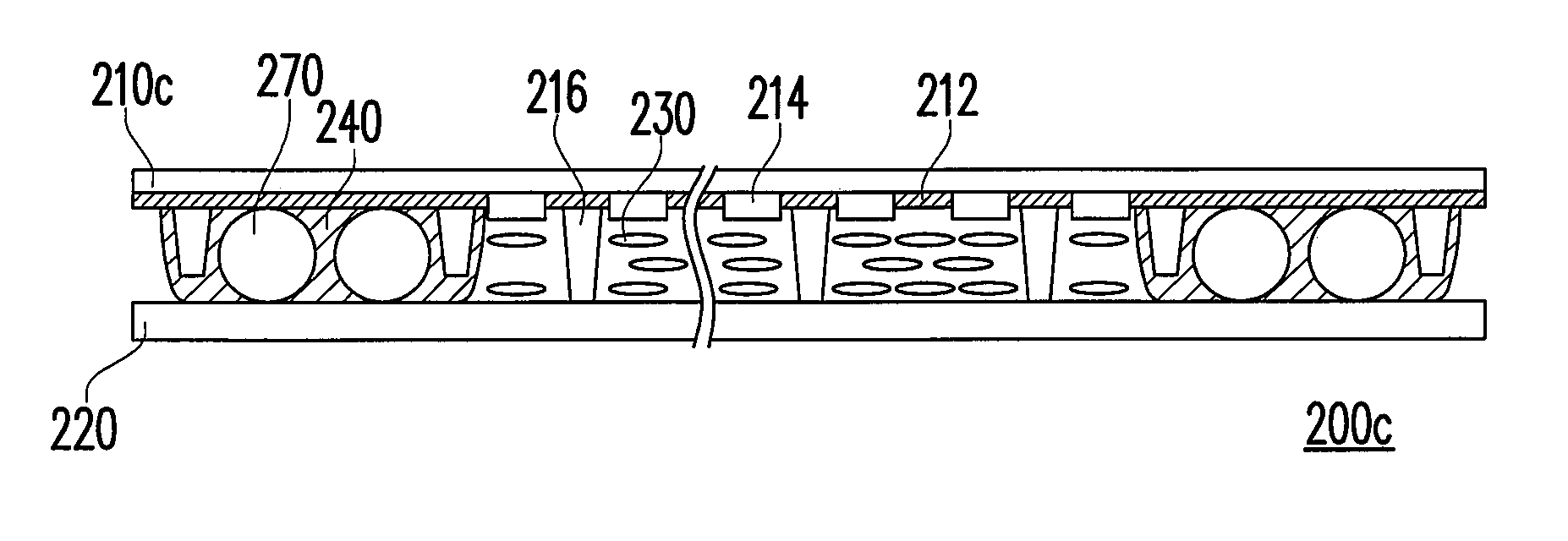
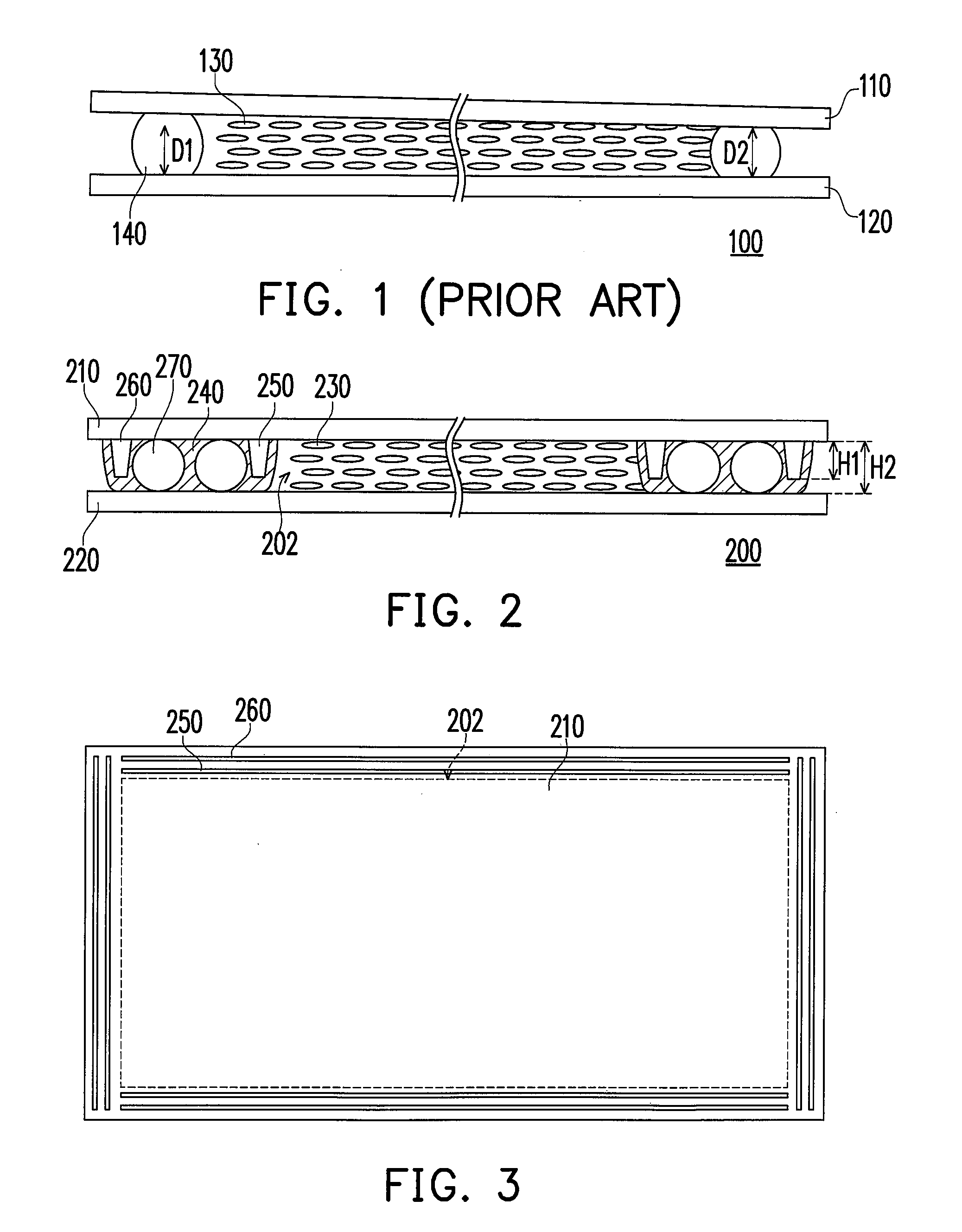
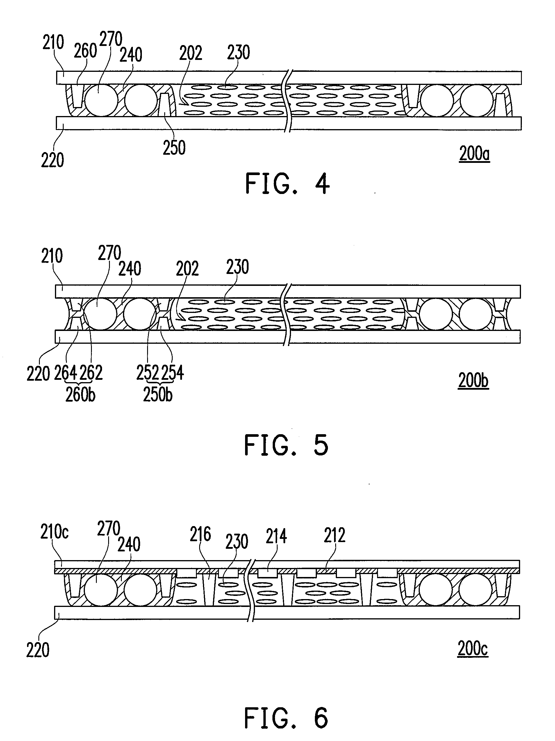
[0033]FIG. 2 is a schematic diagram showing an LCD panel in one embodiment of the invention, and FIG. 3 is a schematic diagram illustrating the first stop structures and the second stop structures on the first substrate in FIG. 2. Referring to FIGS. 2 and 3, the LCD panel 200 of the present embodiment includes a first substrate 210, a second substrate 220, a liquid crystal layer 230, a patterned sealant 240, several first stop structures 250, several second stop structures 260 and several seal spacers 270. The first substrate 210 is opposite to the second substrate 220. The liquid crystal layer 230 and the patterned sealant 240 are disposed between the first substrate 210 and the second substrate 220, and the liquid crystal layer 230 is surrounded by the patterned sealant 240. Further, the first stop structures 250 are disposed inside the patterned sealant 240, and surround the liquid crystal layer 230. The second stop structures 260 are disposed inside the patterned sealant 240 and...


PUM


Abstract

A liquid crystal display (LCD) panel, including a first substrate, a second substrate, a liquid crystal layer, a patterned sealant, several first stop structures, several second stop structures and several seal spacers, is provided. The first substrate is opposite to the second substrate. The liquid crystal layer and the patterned sealant surrounding it are disposed between the first substrate and the second substrate. The first stop structures disposed inside the patterned sealant surround the liquid crystal layer. Each second stop structure disposed inside the patterned sealant is located next to one of the first stop structures. The height H1 of each first or second stop structure is smaller than the distance H2 between the first and second substrates. The seal spacers are disposed inside the patterned sealant and located between the first and the second stop structures. A manufacture method of the LCD panel thereof is further provided.

Description

CROSS-REFERENCE TO RELATED APPLICATION[0001]This application claims the priority benefit of Taiwan application serial no. 95142538, filed Nov. 17, 2006. All disclosure of the Taiwan application is incorporated herein by reference.BACKGROUND OF THE INVENTION[0002]1. Field of the Invention[0003]The present invention relates to a display device, especially to a liquid crystal display panel (LCD panel) and a manufacture method thereof.[0004]2. Description of Related Art[0005]The rapid development of the multi-media society mostly results from the fact that the semiconductor element or the display device has progressed by leaps and bounds. Taking the display device for an example, the cathode ray tube (CRT) has enjoyed the monopoly of the display device market in recent years due to its excellent display quality and low cost. However, the CRT still creates many problems for its occupation of large space and high power consumption. The CRT cannot effectively meet the demands on features s...

Claims


Application Information

Patent Timeline
Patent Type & Authority Applications(United States)
IPC IPC(8): H01L33/00H01L21/30
CPCG02F1/1339G02F2001/13396G02F1/13394G02F1/13396
Inventor WENG, CHIH-HSIUNGCHANG, CHIH-CHIEHWU, PIN-CHUNCHANG, TSUNG-YUAN
Owner AU OPTRONICS CORP
Why Eureka
Try Eureka