Display device and manufacturing method of display device

a display device and manufacturing method technology, applied in the direction of discharge tube luminescnet screens, discharge tube/lamp details, electric discharge lamps, etc., can solve the problems of low reliability, low reliability, and limited practical application, so as to enhance the reliability of the display device, prevent moisture, and high reliability

Active Publication Date: 2008-05-22
SEMICON ENERGY LAB CO LTD
View PDF18 Cites 48 Cited by
  • Summary
  • Abstract
  • Description
  • Claims
  • Application Information

AI Technical Summary

Benefits of technology

[0092]By adopting the structures of the present invention, the effect as shown below can be obtained.
[0093]By providing a sealing film, an interlayer insulating film including an organic material of the display device (panel) is no longer exposed directly to the atmosphere outside of the display device. Therefore, it becomes possible to prevent moisture and oxygen outside of the display device from entering an inside of the display device through an insulating film and the like including a hygroscopic organic material. Accordingly, various degradations such as contamination of an inner part of the display device caused by moisture and oxygen, the degradation of electric properties, a dark spot and shrink can be prevented to enhance reliability of the display device.
[0094]In addition, a display device of high reliability can be manufactured without increasing manufacturing steps because a film made of the same material as that of a film forming the display device is formed at the same time to be used for a sealing film.
[0095]A display device formed like above obtains sufficient operation properties and reliability, because of having a structure in which contaminated materials are shut off in a sealing region in an end part of the display device. Accordingly, an electric appliance using a display device of the present invention also obtains high reliability.

Problems solved by technology

However, after driving a certain period of time, an organic EL element using an organic material for the EL element has a problem in that light-emitting characteristics such as luminance and luminance uniformity degrade drastically compared to those at the beginning.
The low reliability is the main factor for the limited practical application.
In the EL display device (panel) using an EL element, the moisture which enters an inner part leads a serious degradation in reliability to cause a dark spot, shrink and a degradation of luminance from a peripheral part of a light-emitting device.

Method used


Image

  • Display device and manufacturing method of display device
  • Display device and manufacturing method of display device
  • Display device and manufacturing method of display device

Examples


embodiment mode 1

[0123]Referring to the figures, an embodiment mode of the present invention will be described in detail.

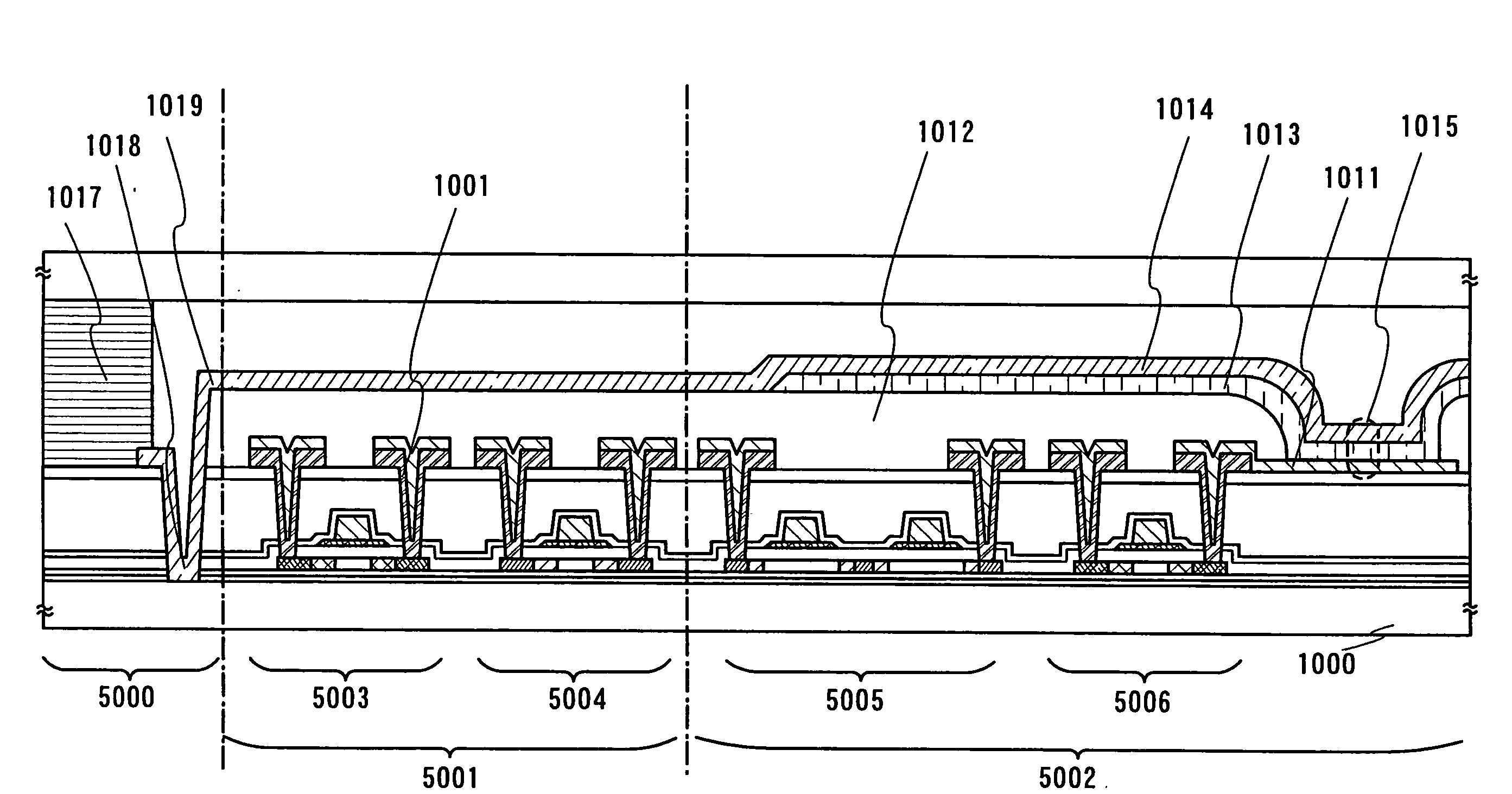
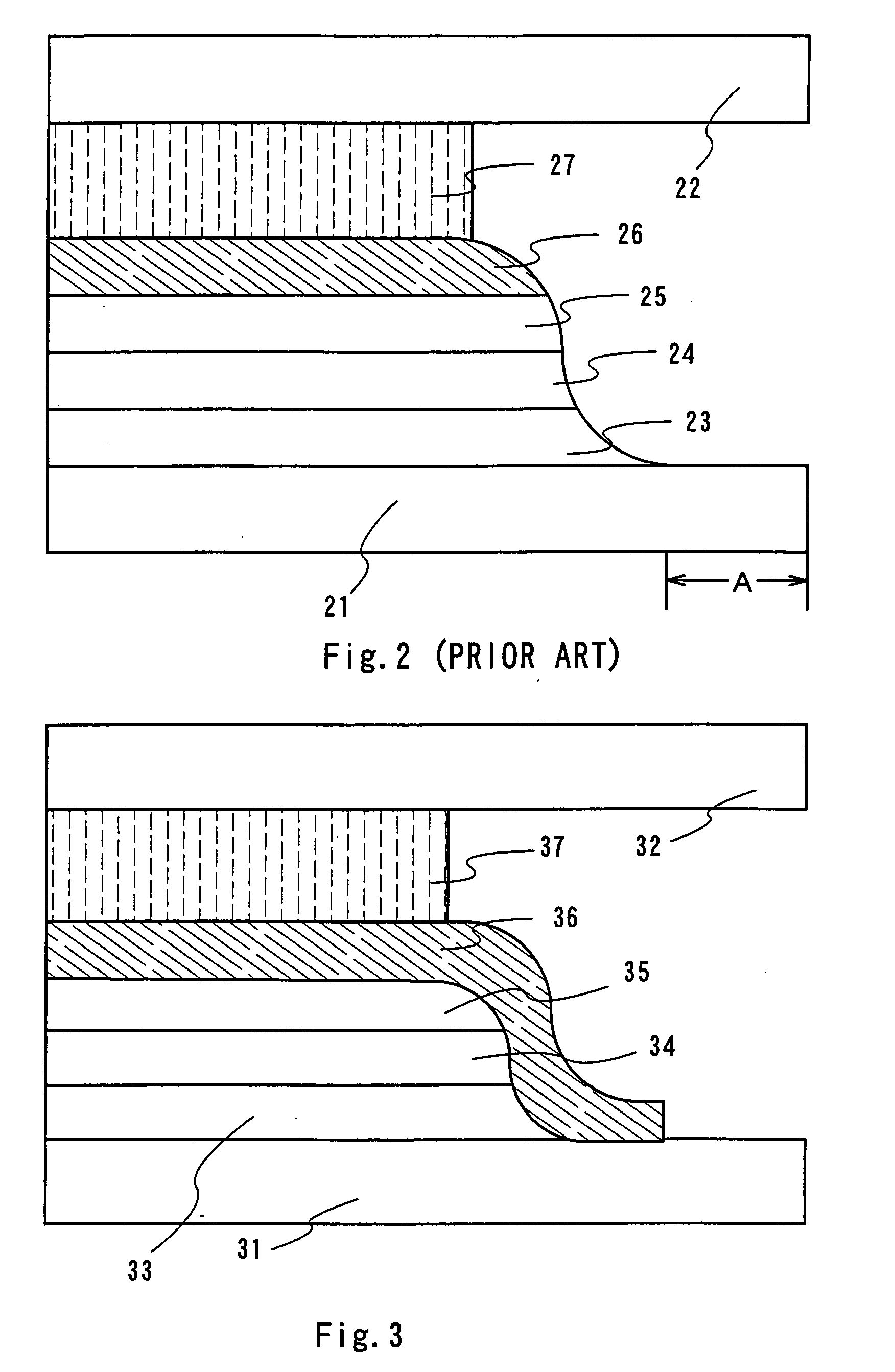
[0124]In a sealing region of a display device, a gate insulating film, an interlayer film and a wiring, which are over a TFT substrate, are stacked to form an insulating layer. In FIG. 3, reference numeral 31 denotes a substrate; 32, a counter substrate; 33, an insulating film; 34 and 35 interlayer films; 36, a sealing film serving as a protective film; 37, a sealing agent. The lamination in FIG. 3 is an example; materials of layers stacked on a TFT substrate side and a sequence of the lamination are not limited to this example. Here, as an example, a display device has a structure in which a base film (not shown in the figure), a gate insulating film, a protective film, an interlayer film and a sealing film are stacked on a glass substrate, having the sealing film on the top of those films.

[0125]As described above, to reduce the area of display device except nonluminescent pixel ...

embodiment mode 2

[0133]An embodiment mode of the present invention is described in detail with reference to the figures.

[0134]In a sealing region of a display device, an insulating film, an interlayer film and a wiring over a TFT substrate are stacked to form an insulating layer. In FIG. 4, reference numeral 41 denotes a substrate; 42, a counter substrate; 43, an insulating film; 44 and 45, interlayer films; 46, a sealing film which serves as a protective film; 47, a sealing agent. The lamination in FIG. 4 is an example; materials of a film stacked on a TFT substrate side and a sequence of the lamination are not limited to this example. Here, as an example, a display device has a structure in which an base film (not shown in the figure), an insulating film, a protective film, and an interlayer film are stacked on a glass substrate, having the sealing film on the top of those films.

[0135]As described before, a sealing agent is applied onto the laminated insulating layer and attaches the substrate inc...

embodiment

Embodiment 1

[0146]The present embodiment describes a method for manufacturing an active matrix substrate with reference to FIGS. 6 to 9. Although an active matrix substrate has plural TFTS, the method for manufacturing the active matrix substrate is described by using a case of having a driving circuit portion including an n-type channel TFT and a p-type TFT, and having a pixel portion.

[0147]As a base film 300, a silicon nitride oxide film is formed on a substrate 200 having an insulating surface in a thickness of 10 to 200 nm (preferably 50 to 100 nm) by a plasma CVD method. A hydrogenated silicon nitride oxide film is then stacked thereon in a thickness of 50 to 200 nm (preferably 100 to 150 nm). In the present embodiment, a 50-nm-thick silicon nitride oxide film and a 100-nm-thick hydrogenated silicon nitride film are formed by a plasma CVD method. As the substrate 200, a glass substrate, a quartz substrate, a silicon substrate, a metal substrate or stainless substrate having an...


PUM


Abstract

In order to provide a display device of high reliability in which an amount of moisture and oxygen, which are a factor for deteriorating a characteristics of a display device, entering from a sealing agent is reduced and its manufacturing method, the present invention has a sealing film. Accordingly, an interlayer insulating film including an organic material of the display device (panel) is no longer exposed to the atmosphere outside of the display device. Therefore, it becomes possible to prevent moisture and oxygen outside of the display device from entering inside of the display device through an insulating film and the like including a hygroscopic organic material. In addition, various degradations such as contamination of an inner part of the display device caused by moisture, oxygen and the like, the degradation of electric properties, a dark spot and shrink can be prevented, thus enhancing reliability of the display device.

Description

TECHNICAL ART[0001]The present invention relates to a display device including an element which has a light-emitting material (hereinafter referred to as light-emitting element) between electrodes (hereinafter referred to as display device) and a manufacturing method thereof. More specifically, the present invention relates to a display device using a light-emitting material in which EL(Electro Luminescence) can be obtained.BACKGROUND ART[0002]Recently, progress has been made in the development of a display device (EL display device) employing a light-emitting element (hereinafter referred to as EL element) which uses EL phenomenon of a light-emitting material. An EL display device does not need a backlight unlike a liquid crystal display because the light-emitting element itself has an ability to emit light. In addition, an EL display device has the advantages of wide viewing angle, high contrast, and so on.[0003]It is said that an EL element emits light by releasing energy when el...

Claims


Application Information

Patent Timeline
Patent Type & Authority Applications(United States)
IPC IPC(8): H05B33/04H01L21/77H01L21/84H01L27/12H01L27/32H01L51/00H01L51/30H01L51/52H05B33/10
CPCH01L27/12H01L27/1214H01L27/3244H01L51/5237H01L51/0062H01L51/0078H01L51/0081H01L51/0052H01L27/127H10K59/12H10K85/649H10K85/615H10K85/311H10K85/324H10K50/841H10K50/844H05B33/04H05B33/10H05B33/14
Inventor TSUCHIYA, KAORUFUKUMOTO, RYOTAMURAKAMI, SATOSHIGODO, HIROMICHI
Owner SEMICON ENERGY LAB CO LTD
Why Eureka
Try Eureka