

Electro-optical device and electronic apparatus having the same
a technology which is applied in the field of optical system and electronic apparatus having the same, can solve the problems of difficult miniaturization of liquid crystal projector, deterioration of liquid crystal properties, and difficult miniaturization of optical system compared to that of liquid crystal device, and achieve excellent reliability and high-quality display
- Summary
- Abstract
- Description
- Claims
- Application Information
AI Technical Summary
Benefits of technology
Problems solved by technology
Method used
Image

Examples
first embodiment
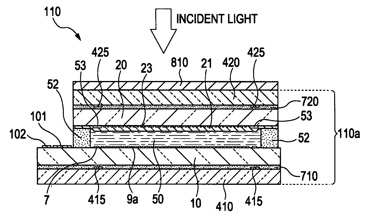
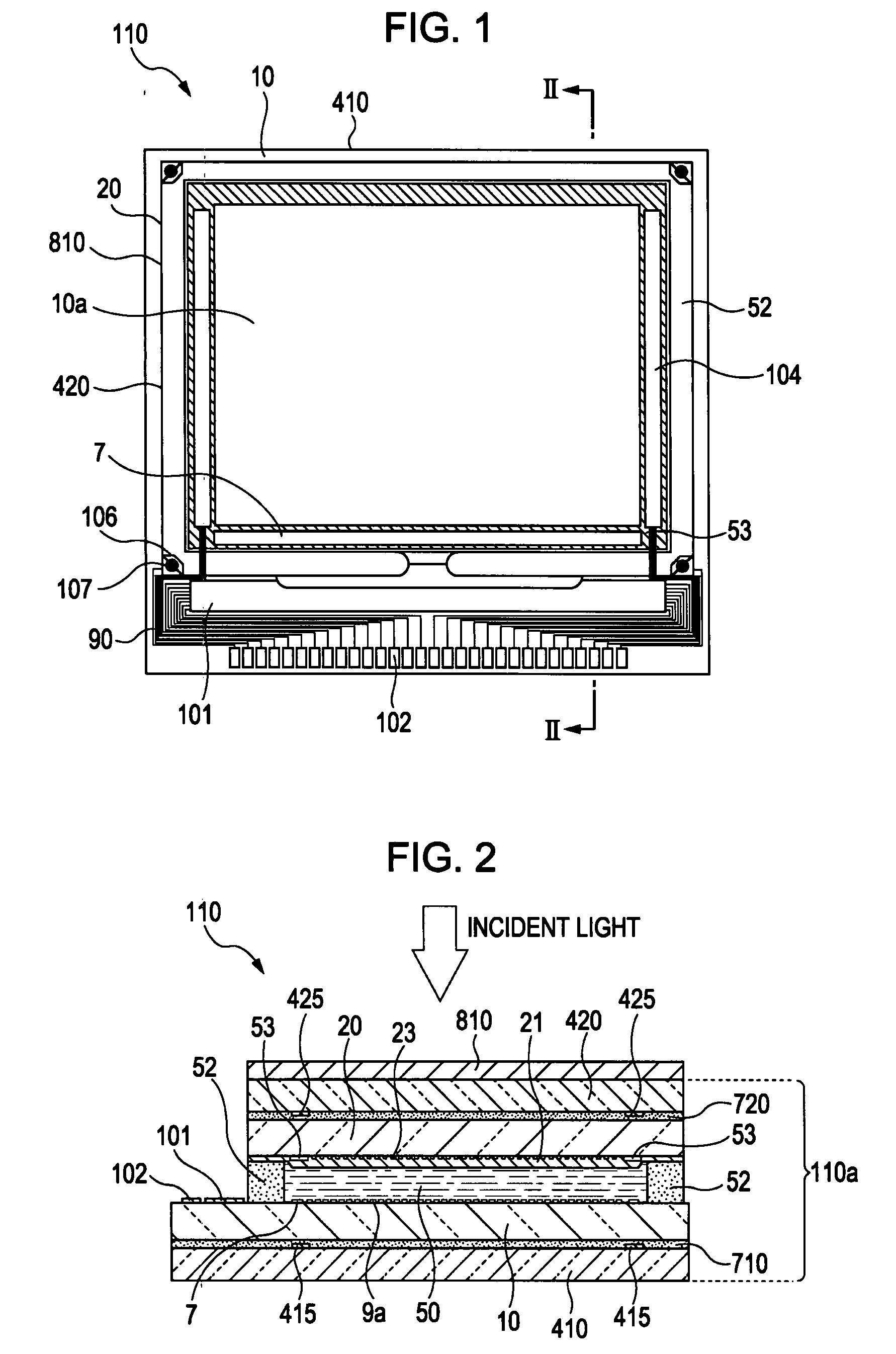
[0037]A liquid crystal device according to a first embodiment will be described with reference to FIGS. 1 to 4. First, the whole structure of the liquid crystal device according to this embodiment will be described with reference to FIGS. 1 and 2. FIG. 1 is a plan view illustrating the whole structure of the liquid crystal device according to this embodiment, and FIG. 2 is a cross-sectional view taken along the line II-II in FIG. 1. In FIG. 2, the individual layers and components are drawn in different scales so that the films and the components can be easily recognized on the drawing.
[0038]In FIGS. 1 and 2, the liquid crystal device 110 according to this embodiment includes a liquid crystal panel 110a and an optical thin film 810 disposed on the surface of the liquid crystal panel 110a at the side on which light is incident. In the liquid crystal device 110 in this embodiment, white light from a light source such as a halogen lamp is incident on the device as incident light from th...
second embodiment
[0057]A liquid crystal device according to a second embodiment will now be described with reference to FIGS. 5 and 6. FIG. 5 is a cross-sectional view of a device according to a second embodiment and corresponds to FIG. 2 in the first embodiment, and FIG. 6 is an enlarged cross-sectional view of an optical thin film according to the second embodiment and corresponds to FIG. 4 in the first embodiment. In FIGS. 5 and 6, the same reference numerals as those in FIGS. 1 to 4 are used for components similar to those in the first embodiment, and their description is optionally omitted.
[0058]The structure of the liquid crystal device 120 according to the second embodiment shown in FIG. 5 is almost the same as that of the liquid crystal device 110 according to the first embodiment except that a liquid crystal panel 120a instead of the liquid crystal panel 110a in the first embodiment and an optical thin film 820 instead of the optical thin film 810 in the first embodiment are used.
[0059]The ...
PUM
 Abstract
Description
Claims
Application Information