Monitoring system for manufacturing semiconductor wafers

Inactive Publication Date: 2008-05-22
CHANG PO CHUN
View PDF2 Cites 1 Cited by
  • Summary
  • Abstract
  • Description
  • Claims
  • Application Information

AI Technical Summary

Benefits of technology

[0007]It is an objective of the present invention to provide a monitoring system for manufacturing semiconductor wafers with a first monitoring picture and a second monitoring picture to effectively determine the status of and bottlenecks in the manufacturing processes.
[0008]It is another objective of the present invention to provide dynamic computer pictures with a predetermined configuration to show the manufacturing status on a display so as to easily control the manufacturing of semiconductors.
[0013]Accordingly, the production supervisor utilizing the monitoring system for manufacturing semiconductor wafers according to the present invention with the first monitoring picture and the second monitoring picture can easily control the manufacturing equipment of the manufacturing processes and determine if there are any bottlenecks in the manufacturing equipment so as to improve the manufacturing efficiency of the semiconductor products, increase the yield rate of the production line and reduce the rework ratio in the factory.

Problems solved by technology

Most of the hardware and software for monitoring the manufacturing processes provides partial process control ability and records detailed production information data and test data with a computer, the production supervisor still cannot effectively determine the actual status with the raw data recorded in the computer without suitable information to show the actual status of the manufacturing process.

Method used


Image

  • Monitoring system for manufacturing semiconductor wafers
  • Monitoring system for manufacturing semiconductor wafers
  • Monitoring system for manufacturing semiconductor wafers

Examples


first embodiment

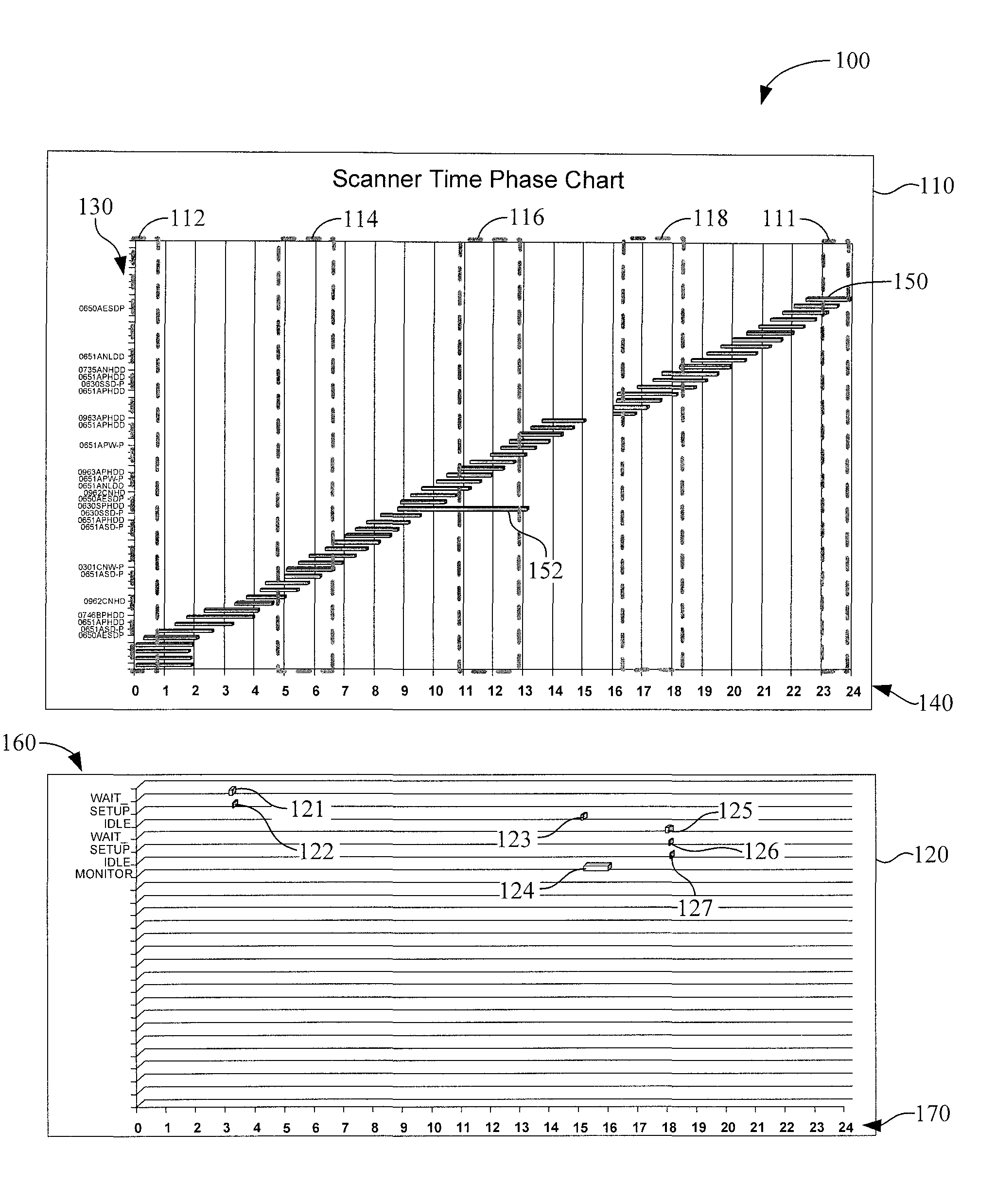
[0022]FIG. 1 illustrates a monitoring system for manufacturing semiconductor wafers according to the present invention. The monitoring system for manufacturing semiconductor wafers 100 includes a first monitoring picture 110 and a second monitoring picture 120, and preferably, the first monitoring picture 110 is disposed above the second monitoring picture 120 and the horizontal coordinates correspond with each other. The horizontal coordinate of the first monitoring picture 110 is preferably a time coordinate 140 and the vertical coordinate is preferably a change record 130. In this embodiment, the change record 130 is preferably a change record for a photo scanner, for example, a photo mask change record such as a change record of photo mask serial numbers. In another embodiment, the change record 130 can be a change record of any tooling, fixtures or jigs in the manufacturing processes. In this embodiment, the horizontal coordinate is a time coordinate 140 and denotes the working...

second embodiment

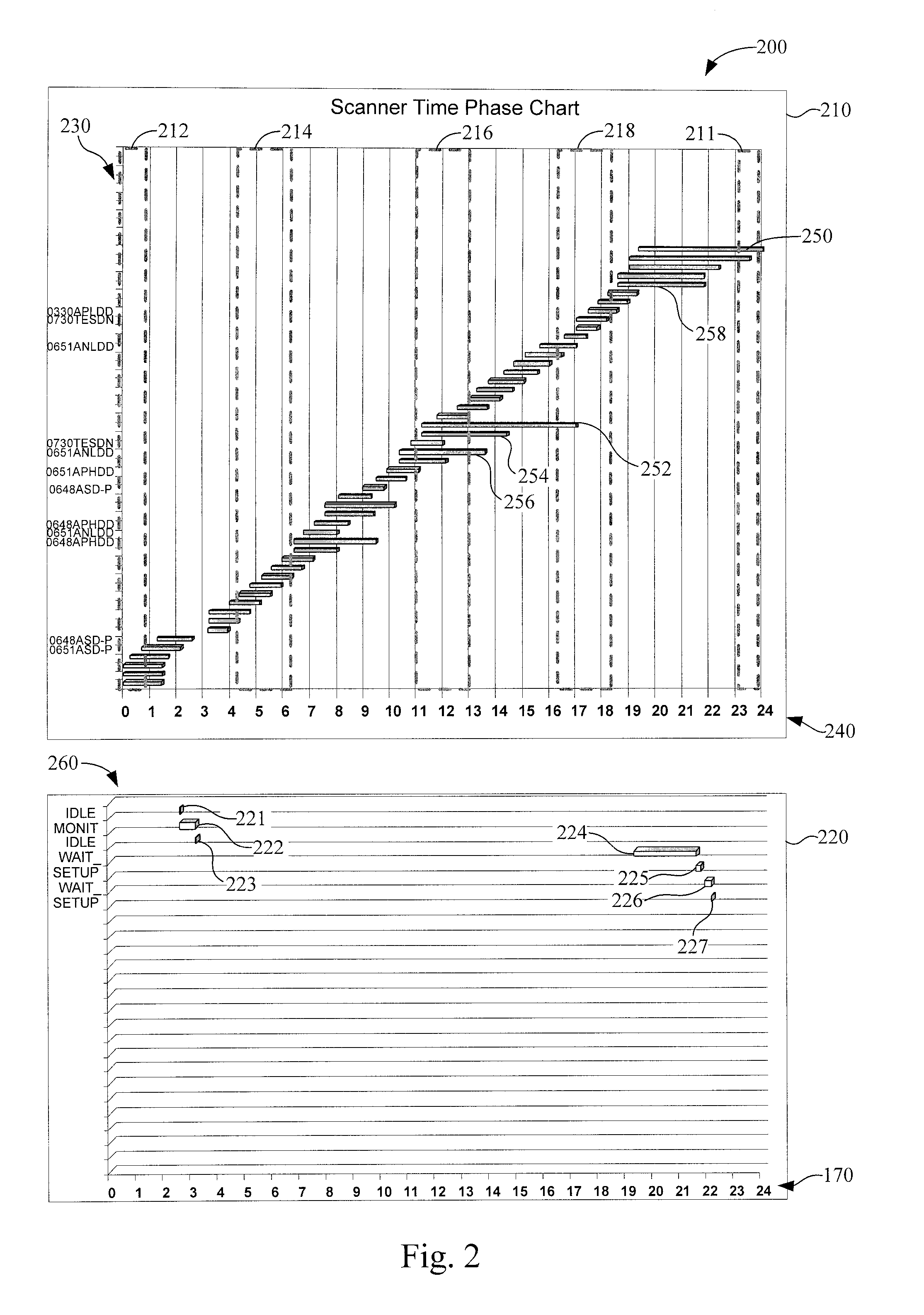
[0029]Referring to FIG. 2, a monitoring system for manufacturing semiconductor wafers according to the present invention is illustrated. The monitoring system for manufacturing semiconductor wafers 200 includes a first monitoring picture 210 and a second monitoring picture 220. Preferably, the first monitoring picture 210 is disposed above the second monitoring picture 220 and the horizontal coordinates thereof correspond with each other. The horizontal coordinate of the first monitoring picture 210 is preferably a time coordinate 240 and the vertical coordinate is preferably a change record 230 such as the photo mask change record 230. Similar to the embodiment of FIG. 1, the change record 230 is preferably a change record for a photo scanner, and therefore the photo mask change record 230 is, for example, a change record of the photo mask serial numbers. The horizontal coordinate is the time coordinate 240 denoting the working time of the photo scanner.

[0030]The first monitoring p...

third embodiment

[0032]Referring to FIG. 3, a monitoring system for manufacturing semiconductor wafers according to the present invention is illustrated. The monitoring system for manufacturing semiconductor wafers 300 also includes a first monitoring picture 310 and a second monitoring picture 320. The horizontal coordinate of the first monitoring picture 310 is preferably a time coordinate 340, and the vertical coordinate thereof is preferably a photo mask change record 330.

[0033]Similarly to FIGS. 1 and 2, this embodiment illustrates the manufacturing information of a photo scanner. Therefore, the vertical coordinate is a photo mask change record 330 and the horizontal coordinate is a time coordinate 340.

[0034]The first monitoring picture 310 utilizes bars 350 to respectively represent the starting manufacture time and ending manufacture time of every wafer lot processed on the photo scanner. A WPH value can also be shown on the first monitoring picture 310, the second monitoring picture 320 or a...


PUM


Abstract

A monitoring system for manufacturing semiconductor wafers is described. The monitoring system includes a first monitoring picture and a second monitoring picture to display manufacture information of a semiconductor manufacture apparatus for the supervisor to judge the efficiency of the apparatus. The first monitoring picture includes a plurality of bars. Each of the bars shows the working time of one wafer lot. The starting point of the bar is the starting manufacture time of the wafer lot and the ending point is the ending manufacture time thereof. The second monitoring picture further includes a plurality of time block to show the status of the apparatus. The starting points of the blocks are the starting time of the status and the ending points are the ending time thereof. The first monitoring picture further includes a plurality of controlling periods.

Description

RELATED APPLICATIONS[0001]This application claims priority to Taiwan Application Serial Number 95142872, filed Nov. 20, 2006, which is herein incorporated by reference.FIELD OF THE INVENTION[0002]The present invention generally relates to a monitoring system for manufacturing semiconductor wafers. More particularly, this invention relates to a monitoring picture of a monitoring system for manufacturing semiconductor wafers.BACKGROUND OF THE INVENTION[0003]Since the semiconductor industry is highly developed, electronic products are becoming increasingly light and the functionalities thereof are increasingly powerful. Nowadays, semiconductor ICs are produced by a plurality of precise manufacturing processes to define the circuits and elements on the wafer.[0004]The precise manufacturing processes are achieved on a lot of manufacturing equipment with numerous manufacturing controls. Therefore, to effectively control the manufacturing of semiconductors, the semiconductor manufacturing ...

Claims


Application Information

Patent Timeline
IPC IPC(8): G06K9/00
CPCG05B23/0267
Inventor CHANG, PO-CHUN
Owner CHANG PO CHUN
Why Eureka
Try Eureka