
Semiconductor chip having bumps of different heights and semiconductor package including the same

Inactive Publication Date: 2008-05-22
SAMSUNG ELECTRONICS CO LTD
View PDF2 Cites 11 Cited by
  • Summary
  • Abstract
  • Description
  • Claims
  • Application Information

AI Technical Summary

Benefits of technology

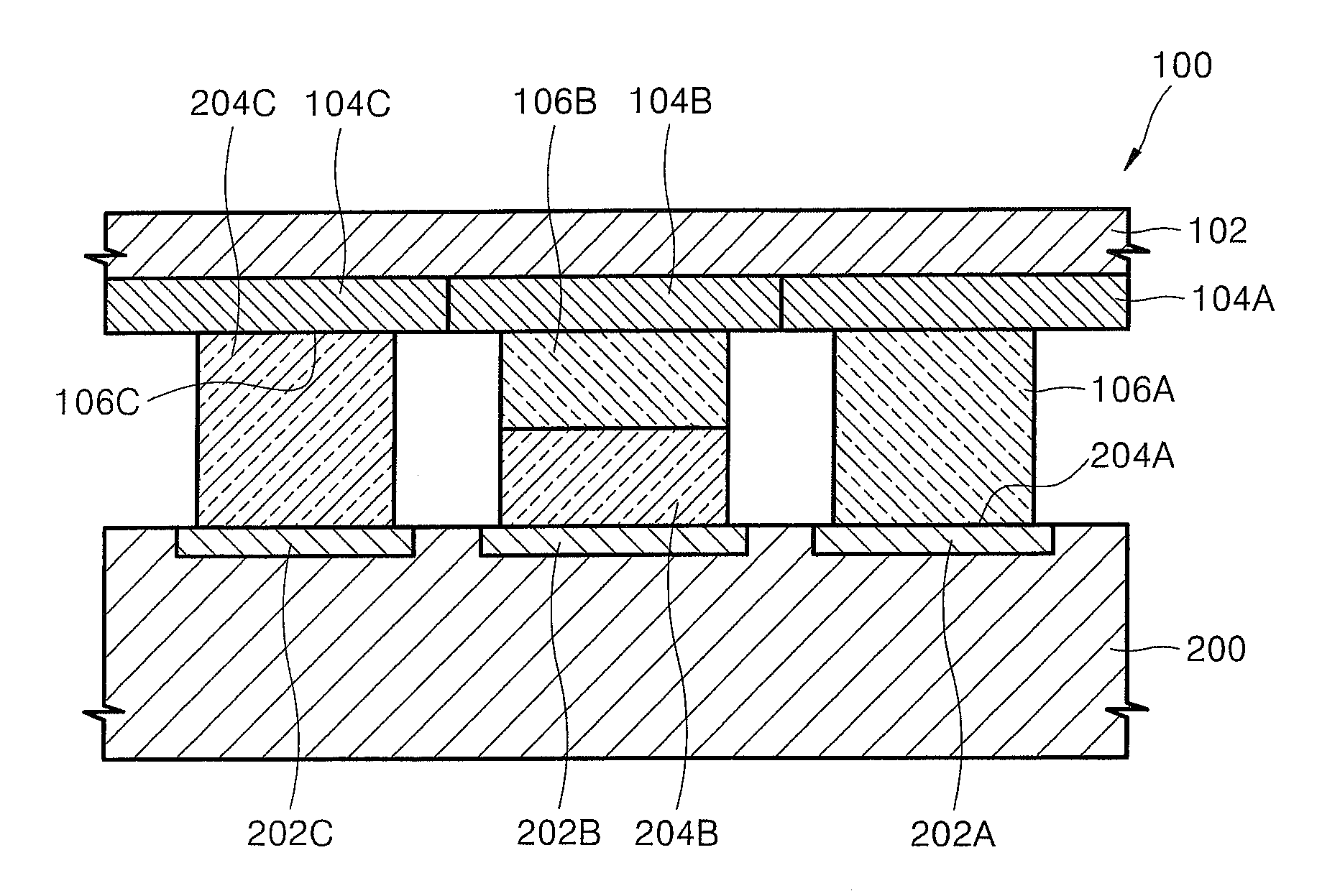
[0012]Embodiments of the invention provide a semiconductor chip having bumps formed with different heights. This configuration allows more dense connection patterns between the semiconductor chip and a corresponding circuit board. In effect, embodiments of the invention arrange bumps and corresponding connection components (e.g., bond pads and / or circuit patterns) in three-dimensions to yield more dense connection arrangements.

Problems solved by technology

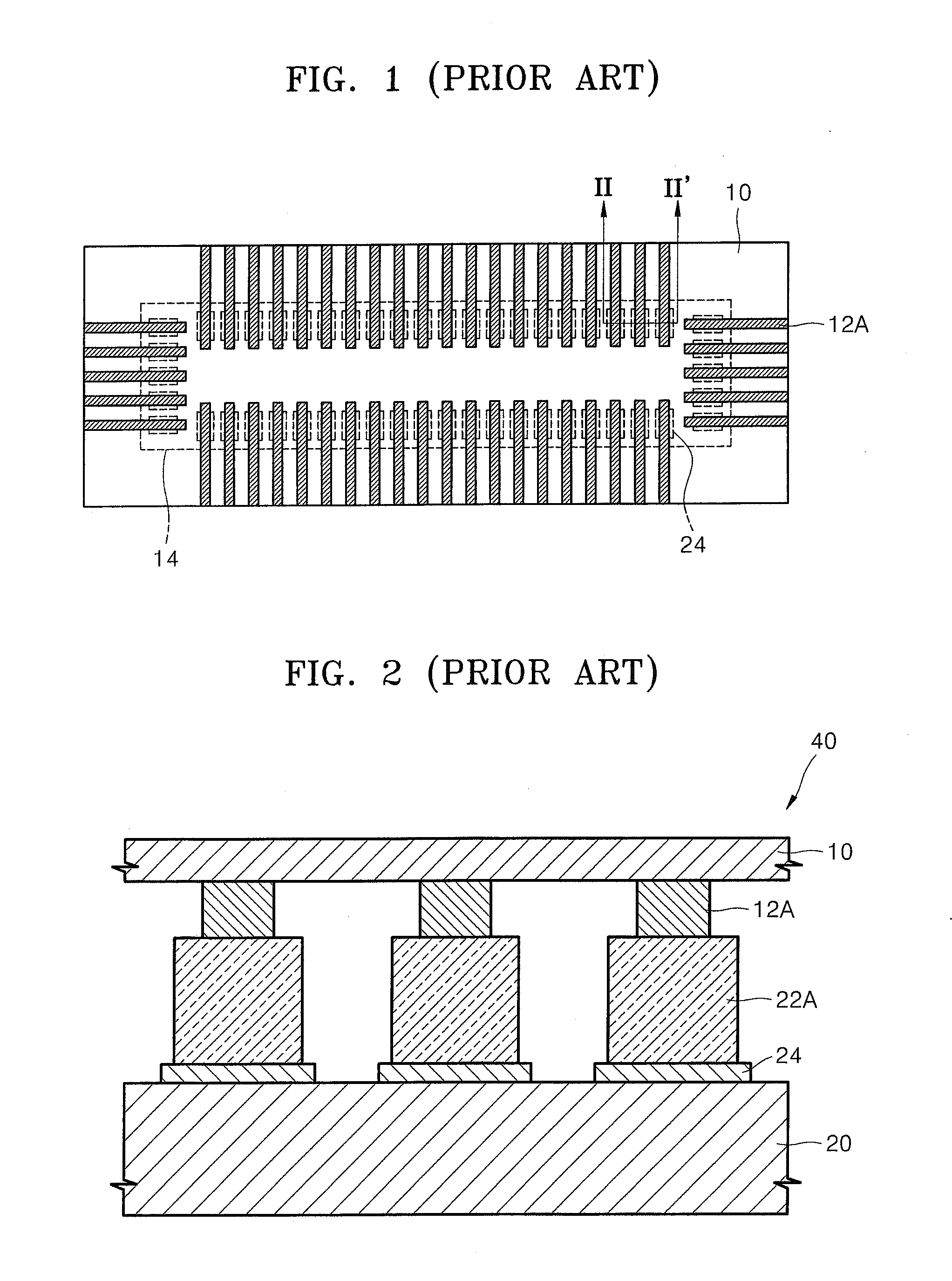
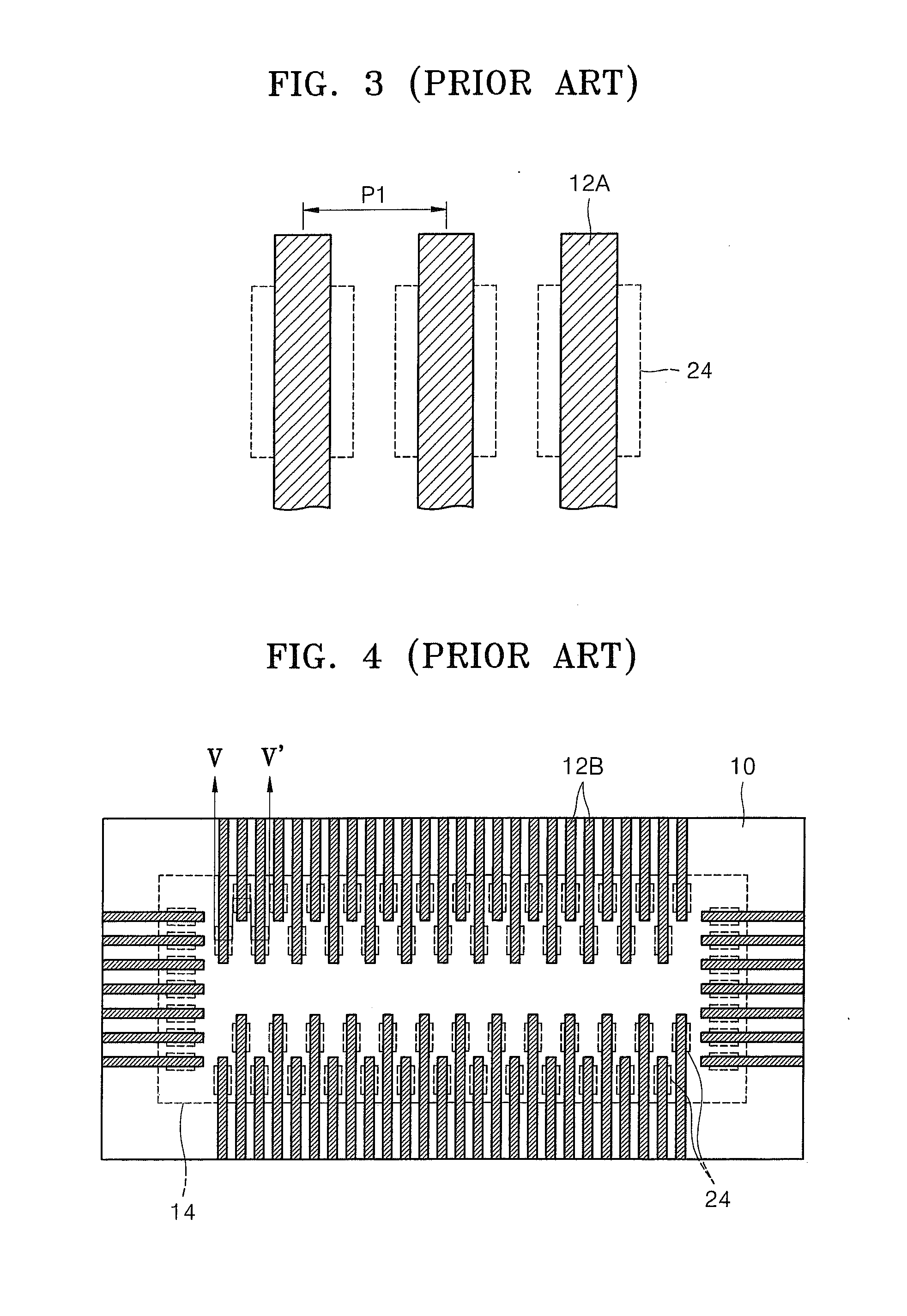
As a result of these fine pitch bonds pads, it has become increasingly difficult to connect semiconductor chips with related circuit boards.
For example, it is difficult to form printed circuit patterns on the circuit board with correspondingly fine pitches, and misalignment problems and short circuit contacts may result during a subsequent assembly process.

Method used


Image

  • Semiconductor chip having bumps of different heights and semiconductor package including the same
  • Semiconductor chip having bumps of different heights and semiconductor package including the same
  • Semiconductor chip having bumps of different heights and semiconductor package including the same

Examples


Embodiment Construction

[0029]Embodiments of the invention will now be described in some additional detail with reference to the accompanying drawings. The invention may, however, be embodied in many different forms and should not be construed as being limited to only the illustrated embodiments. Rather, the embodiments are provided as teaching examples.

[0030]FIG. 7 is a plan view of a film 10 adapted to mount one or more semiconductor chips using conventional chip on film (COF) packaging techniques. Film 10 of FIG. 7 is shown in a state where it is prepared to receive a semiconductor chip. Film 10 is illustrated in the form of a conventional COF package, film 10 being formed from polyimide or some similar material having a superior thermal expansion coefficient or great durability. However, the scope of the invention is not limited to COF packages, but may be more broadly applied across a range of semiconductor packaging. A chip mounting area 14 on film 10 is provided to receive one or more semiconductor ...


PUM


Abstract

A semiconductor chip is disclosed and includes a plurality of bond pads disposed on a semiconductor chip, and a plurality of chip bumps of different heights disposed on a corresponding bond pad.

Description

CROSS-REFERENCE TO RELATED PATENT APPLICATIONS[0001]This application claims the benefit of Korean Patent Application No. 10-2006-0115430, filed on Nov. 21, 2006, the subject matter of which is hereby incorporated by reference.BACKGROUND OF THE INVENTION[0002]1. Field of the Invention[0003]The present invention relates to a semiconductor chip and a semiconductor package including the same. More particularly, the invention relates to a semiconductor chip adapted for connection to a circuit board through bumps and a semiconductor package including the semiconductor chip.[0004]2. Description of the Related Art[0005]As contemporary semiconductor chips have become increasing small in size, the constituent bond pads used to connect such semiconductor chips have been implemented with ever finer pitches. As a result of these fine pitch bonds pads, it has become increasingly difficult to connect semiconductor chips with related circuit boards. For example, it is difficult to form printed circ...

Claims


Application Information

Patent Timeline
IPC IPC(8): H01L23/48H05K1/00
CPCH01L23/49572H01L2924/014H01L24/73H01L24/81H01L2224/13016H01L2224/13099H01L2224/13144H01L2224/81136H01L2224/81801H01L2924/01015H01L2924/01029H01L2924/01033H01L2924/01074H01L2924/01079H01L2924/01082H05K1/189H05K3/303H05K3/3436H05K2201/0367H05K2201/094H05K2201/09709H05K2201/10674H05K2201/10681H05K2203/167H01L2924/01006H01L2924/01023H01L24/16H01L2224/0554H01L2224/05567H01L2224/05568H01L2224/05573H01L2224/13017H01L2224/13019H01L2224/81193H01L2924/00014Y02P70/50H01L2224/05599H01L2224/0555H01L2224/0556H01L23/48
Inventor HWANG, JI-HWANKIM, DONG-HANKIM, CHUL-WOOLEE, SANG-HEUIBAE, KWANG-JIN
Owner SAMSUNG ELECTRONICS CO LTD
Learn More