Ge short wavelength infrared imager

a short wavelength infrared and imager technology, applied in the field of integrated circuits and semiconductor processes, can solve the problems of small inp substrates (only up to 4 inches in diameter), high cost of fabricating epitaxial ingaas films on inp substrates, and high cost of cameras based on these image sensors

Active Publication Date: 2008-05-29
SHARP KK AKA SHARP CORP +1
View PDF5 Cites 80 Cited by
  • Summary
  • Abstract
  • Description
  • Claims
  • Application Information

AI Technical Summary

Benefits of technology

[0015]A Si CMOS read-out circuit on Si wafers is prepared using any standard, state-of-the-art process. The pitch of the read-out circuit matches that of the Ge FPA, and the circuit design keeps the two terminals of each Ge photodetector at nearly zero relative bias, preferably less than 0.001V.
[0016]Using any state-of-the-art flip-chip bonding process, the Ge FPA is bonded to the Si CMOS read-out circuit. The fabrication of the back-side illuminated imager is completed using any state-of-the-art packaging and necessary low-noise amplifier and digital processing circuitry.
[0017]Accordingly, a germanium (Ge) short wavelength infrared (SWIR) imager is provided. The imager comprises a silicon (Si) substrate with doped wells. An array of pin diodes is formed in a relaxed Ge-containing film overlying the Si substrate, each pin diode having a flip-chip interface. There is a Ge/Si interface, and a doped Ge-containing buffer layer interposed between the Ge-containing film and the Ge/Si interface. An array of Si CMOS readout circuits is bonded to the flip-chip interfaces. Each readout circuit has a zero volt diode bias interfac

Problems solved by technology

Compared to Si substrates, InP substrates are small (only up to 4 inches in diameter), fragile, and very expensive.
However, due to the small size and fragility of available InP substrates, the cost of fabricating epitaxial InGaAs films on InP substrates is very high.
This, in turn, keeps the cost of cameras based on these image sensors very expe

Method used


Image

  • Ge short wavelength infrared imager
  • Ge short wavelength infrared imager
  • Ge short wavelength infrared imager

Examples


Embodiment Construction

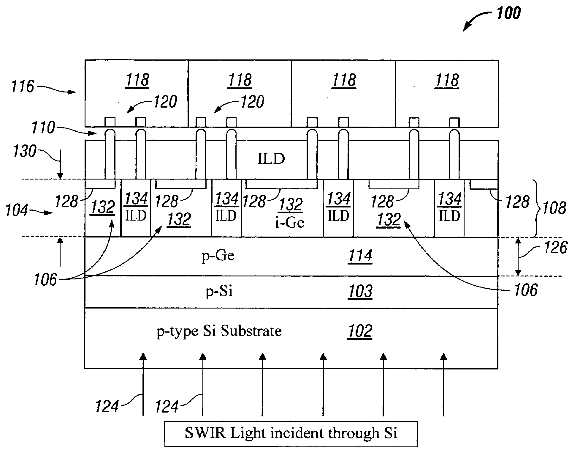
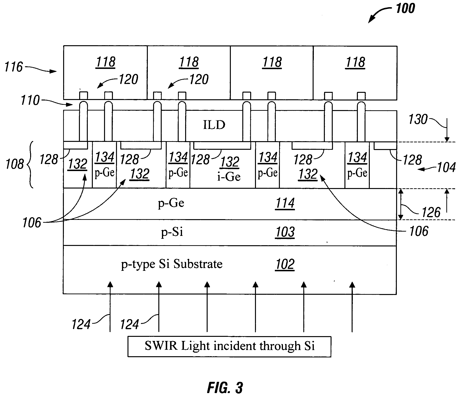
[0029]FIG. 1 is a partial cross-sectional view of a germanium (Ge) short wavelength infrared (SWIR) imager. The imager 100 comprises a silicon (Si) substrate 102 with doped wells 103. Here, a p-type Si substrate 102 is shown with a single p-doped well 103 for simplicity. But it should be understood that a substrate may be made up of a plurality of wells. Likewise, a doping design based upon a p-type substrate is shown, but it should be understood that an equivalent design could be enabled with an n-type substrate (or large n-doped well in a p-substrate).

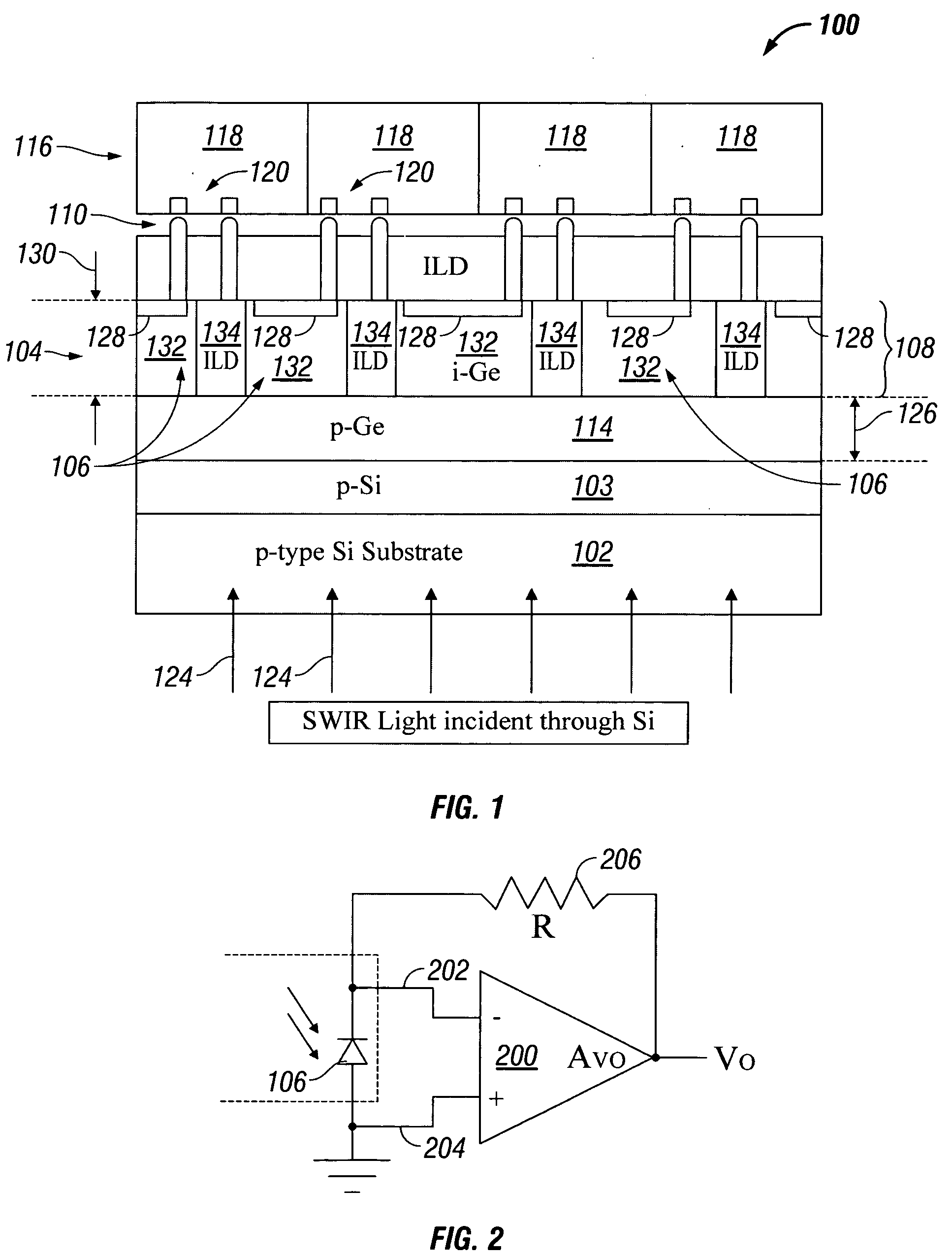
[0030]An array 104 of pin diodes 106 is formed in a relaxed Ge-containing film 108 overlying the Si substrate 102. For example, the Ge-containing film 108 may be Ge, SiGe, or graded SiGe. Each pin diode 106 has a flip-chip interface 110. Only a row of 4 diodes 106 is shown in the figure, however, it should be understood that the array may include any large number of diodes arranged in a matrix of rows and column.

[0031]A Ge / Si interfa...


PUM


Abstract

A germanium (Ge) short wavelength infrared (SWIR) imager and associated fabrication process are provided. The imager comprises a silicon (Si) substrate with doped wells. An array of pin diodes is formed in a relaxed Ge-containing film overlying the Si substrate, each pin diode having a flip-chip interface. There is a Ge/Si interface, and a doped Ge-containing buffer interposed between the Ge-containing film and the Ge/Si interface. An array of Si CMOS readout circuits is bonded to the flip-chip interfaces. Each readout circuit has a zero volt diode bias interface.

Description

BACKGROUND OF THE INVENTION[0001]1. Field of the Invention[0002]This invention generally relates to integrated circuit (IC) and semiconductor processes and, more particularly, to a germanium (Ge) short wavelength infrared (SWIR) imager and associated fabrication process.[0003]2. Description of the Related Art[0004]Short wavelength infrared (SWIR) imagers, with about a 1 to 1.7 micron wavelength, are used in camera systems for military and security night vision applications, as well as in many machine vision applications. Most conventional SWIR light-sensitive components are made of InGaAs films epitaxially grown on InP substrates. Compared to Si substrates, InP substrates are small (only up to 4 inches in diameter), fragile, and very expensive.[0005]By adjusting the relative In and Ga content, the lattice constant of InGaAs can be tailored to match the InP lattice constant, or be very close to it, thus minimizing threading dislocations and the accompanying increase in dark current. ...

Claims


Application Information

Patent Timeline
IPC IPC(8): H01L31/028H01L31/18
CPCH01L27/14643H01L31/1055H01L27/14689H01L27/14649
Inventor TWEET, DOUGLAS J.MAA, JER-SHENLEE, JONG-JANHSU, SHENG TENG
Owner SHARP KK AKA SHARP CORP
Why Eureka
Try Eureka