Resistive random access memory and method of manufacturing the same

a random access memory and resistive technology, applied in the field of resistive random access memory, can solve the problems of slow operation speed, lower integration and speed of resistive memory, and increased market competitiveness, and achieve the effect of stabilizing voltage and resistance variations

Active Publication Date: 2008-05-29
SAMSUNG ELECTRONICS CO LTD
View PDF43 Cites 24 Cited by
  • Summary
  • Abstract
  • Description
  • Claims
  • Application Information

AI Technical Summary

Benefits of technology

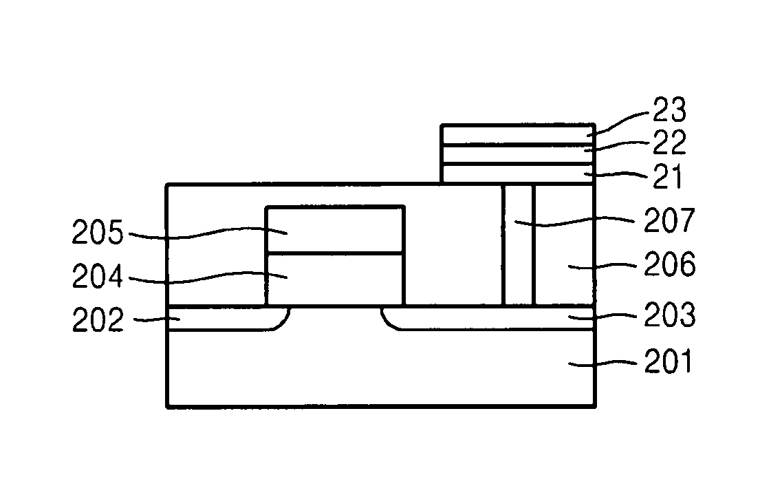
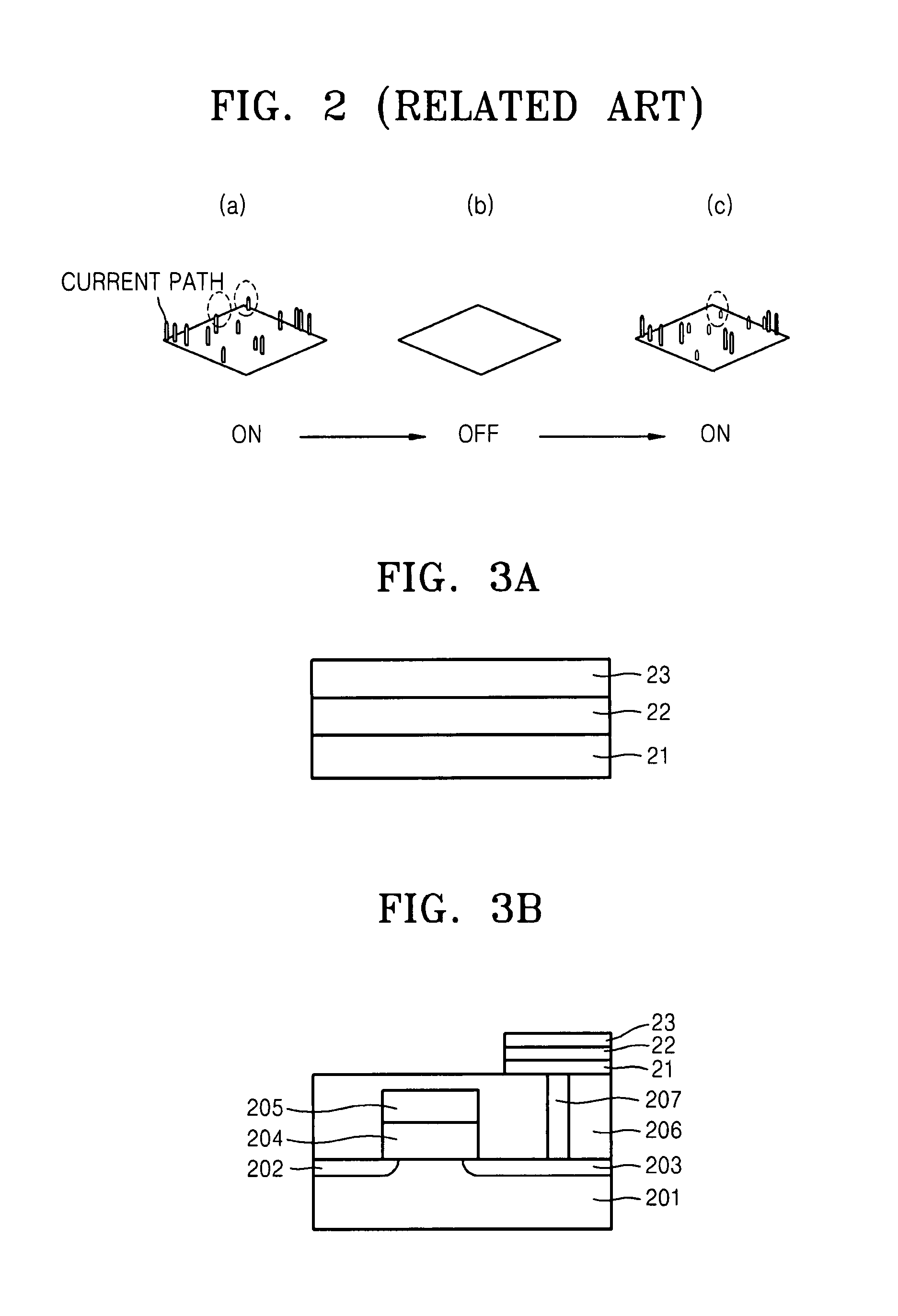
[0011]Example embodiments provide a resistive random access memory (RRAM) having a structure capable of stabilizing a reset current and a set voltage using a resistance varying material and a method of manufacturing the RRAM. The RRAM may include a resistive layer having a metal dopant so as to form a filament as a current path in the resistive layer, thus stabilizing voltage and resistance variations.

Problems solved by technology

On the other hand, a flash memory may be representative of a non-volatile memory capable of preserving stored data when the power is turned off (unlike a volatile memory) but may have lower integration and slower operating speeds than a DRAM.
However, where a conventional DRAM process is used to manufacture the PRAM, etching may be more difficult and may require a longer period of time.
Consequently, market competitiveness may be decreased.
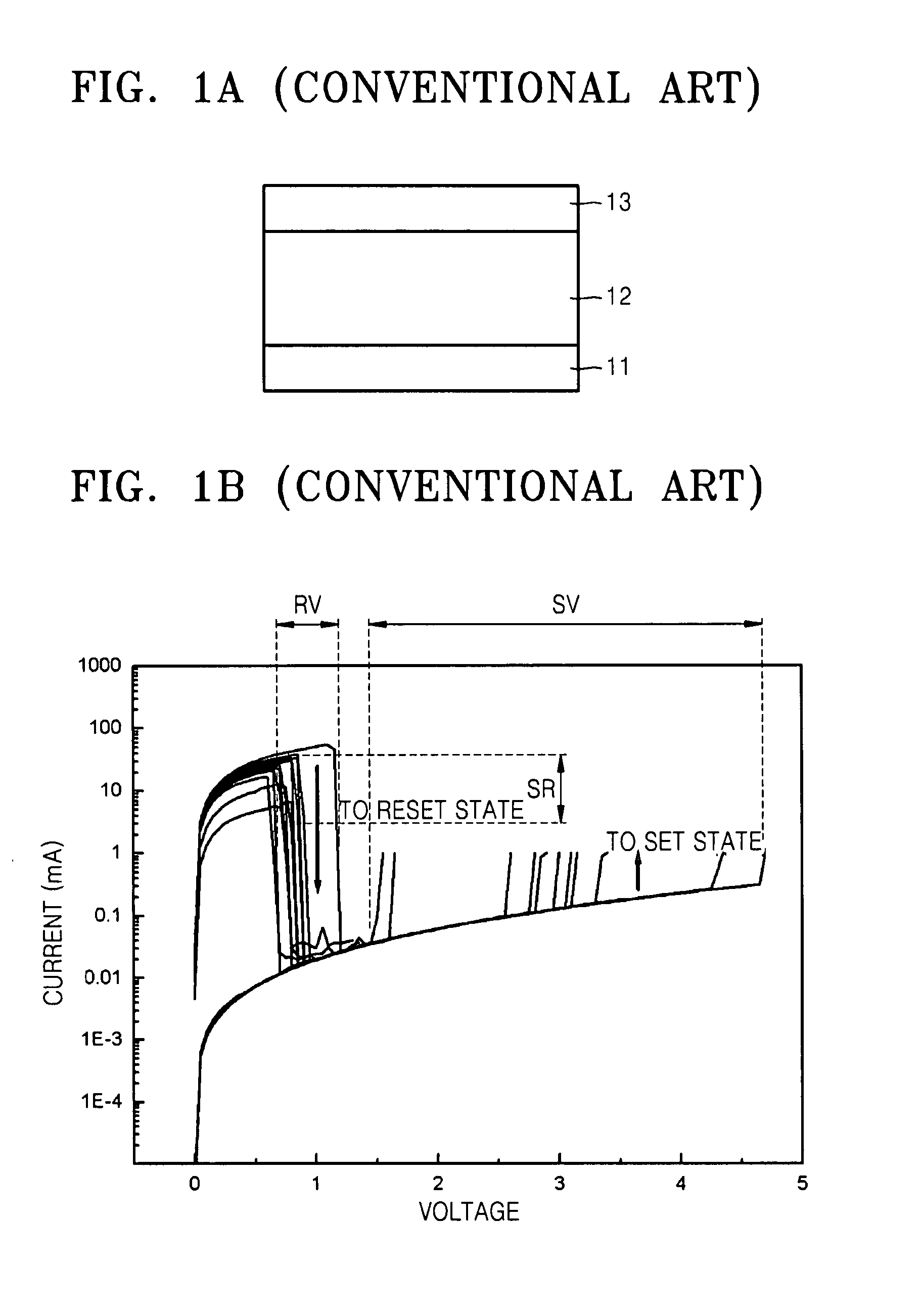
Because the current path in the resistive layer 12 may not be uniform with the driving of the conventional RRAM (and thus the resistance level may be relatively unstable), the conventional RRAM may have larger voltage and resistance variations.
Consequently, the set and reset voltages of the conventional RRAM may be relatively unstable, thus lowering reliability.

Method used


Image

  • Resistive random access memory and method of manufacturing the same
  • Resistive random access memory and method of manufacturing the same
  • Resistive random access memory and method of manufacturing the same

Examples


Embodiment Construction

[0025]A resistive random access memory (RRAM) and a method of manufacturing the RRAM according to example embodiments will now be described with reference to the attached drawings. In the drawings, the thicknesses of layers and regions may have been exaggerated for clarity.

[0026]It will be understood that when an element or layer is referred to as being “on”, “connected to”, “coupled to”, or “covering” another element or layer, it may be directly on, connected to, coupled to, or covering the other element or layer or intervening elements or layers may be present. In contrast, when an element is referred to as being “directly on,”“directly connected to” or “directly coupled to” another element or layer, there are no intervening elements or layers present. Like numbers refer to like elements throughout. As used herein, the term “and / or” includes any and all combinations of one or more of the associated listed items.

[0027]It will be understood that, although the terms first, second, th...


PUM


Abstract

Example embodiments relate to a resistive random access memory (RRAM) and a method of manufacturing the RRAM. A RRAM according to example embodiments may include a lower electrode, which may be formed on a lower structure (e.g., substrate). A resistive layer may be formed on the lower electrode, wherein the resistive layer may include a transition metal dopant. An upper electrode may be formed on the resistive layer. Accordingly, the transition metal dopant may form a filament in the resistive layer that operates as a current path.

Description

PRIORITY STATEMENT[0001]This application claims priority under 35 U.S.C. §119 to Korean Patent Application No. 10-2006-0118560, filed on Nov. 28, 2006 in the Korean Intellectual Property Office (KIPO), the entire contents of which are incorporated herein by reference.BACKGROUND[0002]1. Technical Field[0003]Example embodiments relate to a resistive random access memory (RRAM) and a method of manufacturing the RRAM.[0004]2. Description of the Related Art[0005]A semiconductor memory array structure may include a plurality of interconnected memory cells. For example, a unit memory cell of a dynamic random access memory (DRAM) may include a switch and a capacitor. A DRAM may have higher integration and faster operating speeds. However, when the power is turned off, all of the stored data may be erased from the DRAM.[0006]On the other hand, a flash memory may be representative of a non-volatile memory capable of preserving stored data when the power is turned off (unlike a volatile memory...

Claims


Application Information

Patent Timeline
Patent Type & Authority Applications(United States)
IPC IPC(8): H01L45/00
CPCH01L27/2436H01L45/085H01L45/165H01L45/146H01L45/1233H10B63/30H10N70/245H10N70/043H10N70/8833H10N70/826G11C13/0004H10N70/023H10N70/026
Inventor SEO, SUN-AEPARK, YOUNG-SOOJUNG, RAN-JULEE, MYOUNG-JAEKIM, DONG-CHULAHN, SEUNG-EON
Owner SAMSUNG ELECTRONICS CO LTD
Why Eureka
Try Eureka