

Layered Semiconductor Wafer With Low Warp And Bow, And Process For Producing It
a technology of semiconductor wafers and layered semiconductors, which is applied in the direction of semiconductor devices, semiconductor/solid-state device details, electrical devices, etc., can solve the problems of serious complications in the fabrication of electronic components, deformation of soi wafers produced by this process, and unplanar surface, etc., to achieve no harmful side effects, simple implementation, and different profile
- Summary
- Abstract
- Description
- Claims
- Application Information
AI Technical Summary
Benefits of technology
Problems solved by technology
Method used
Image

Examples
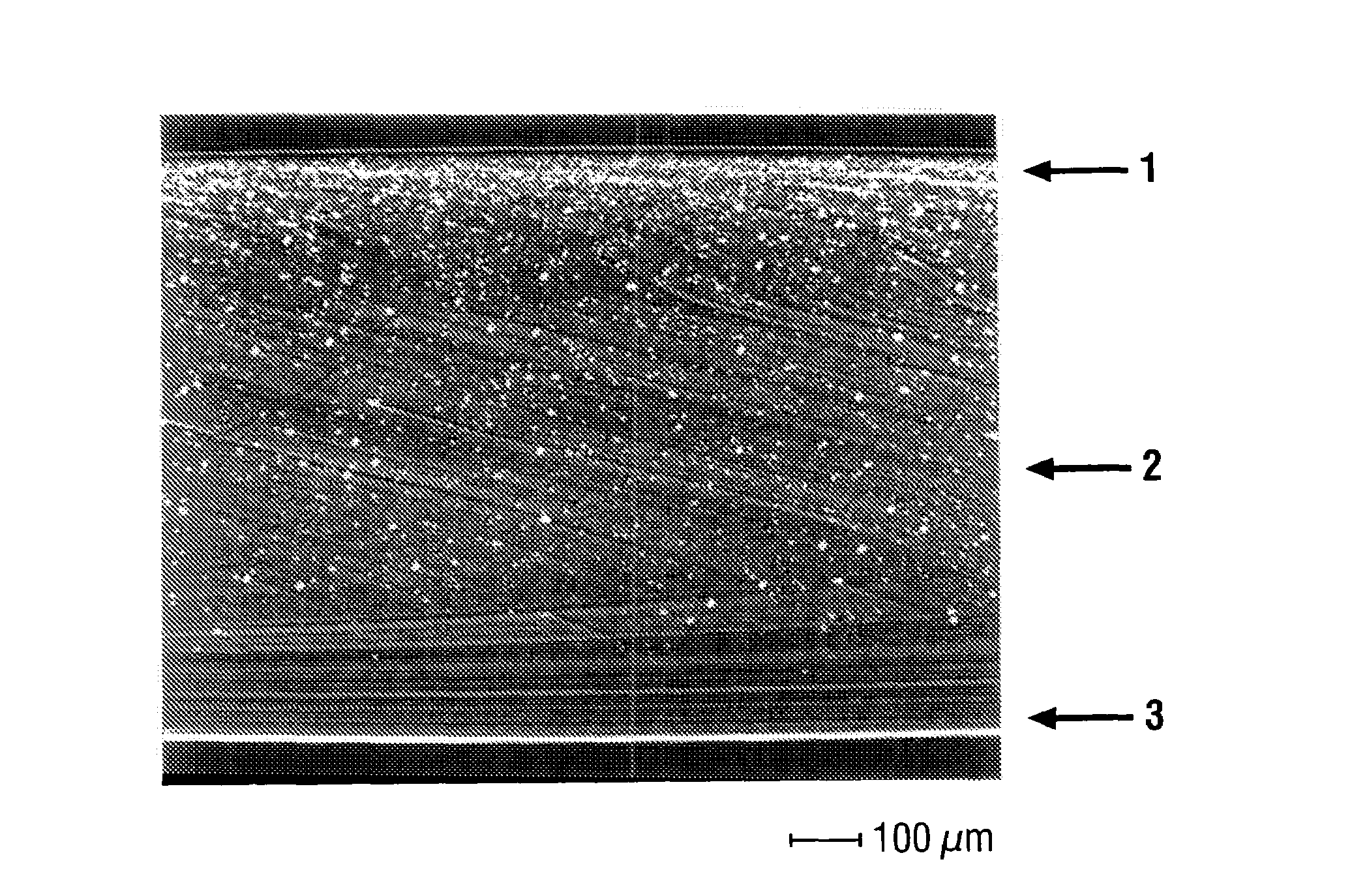
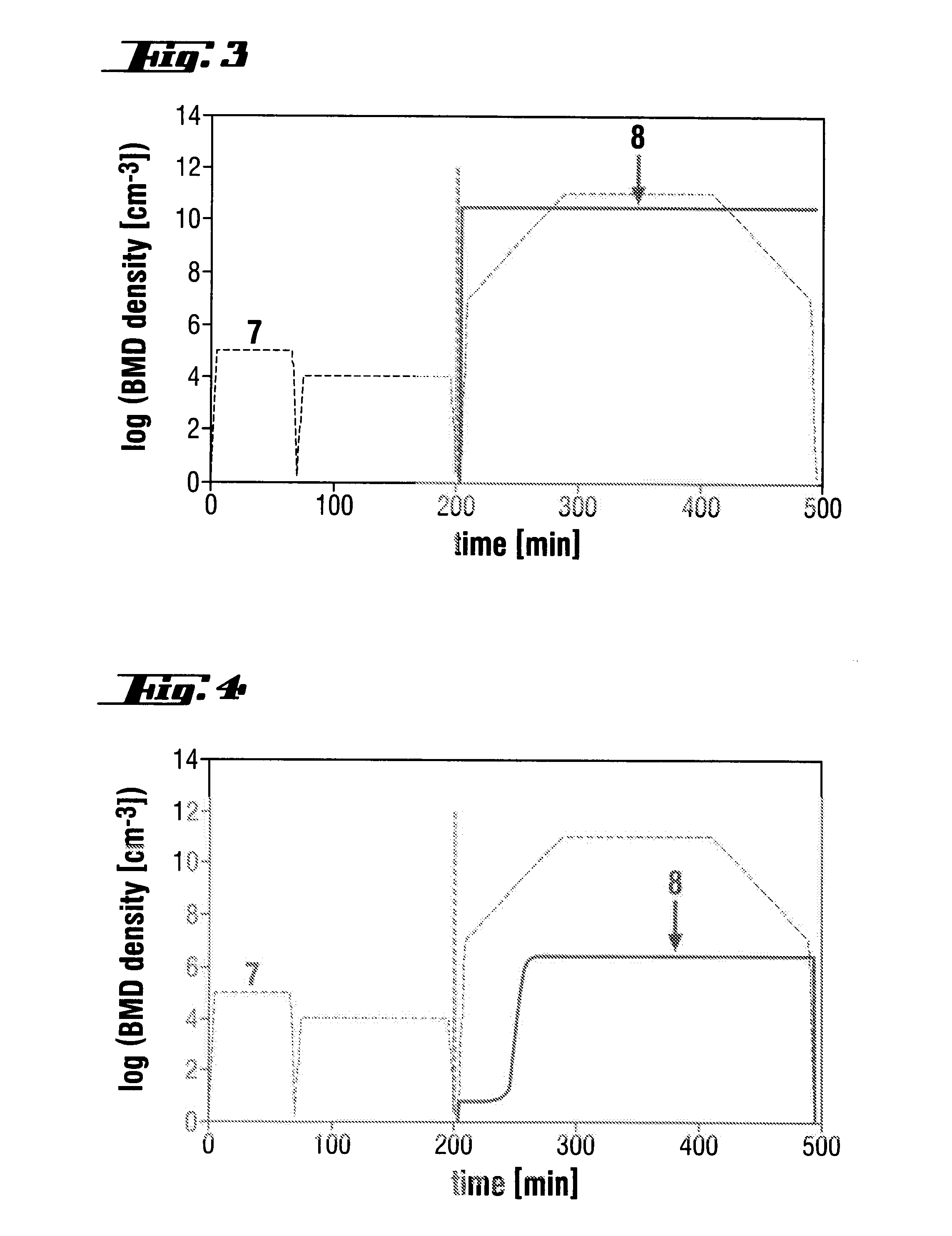
example 1a
[0042]The RTA treatment was carried out in a nitrogen atmosphere in accordance with the first process according to the invention. The RTA treatment was carried out in a single stage at a heating rate of 100° C. / s to 1,200° C. The SOI wafer was then held at this temperature for 10 s and then cooled to room temperature at a cooling rate of 15° C. / s.
example 1b
[0043]The RTA treatment was carried out in a nitrogen atmosphere in accordance with the first process according to the invention. The RTA treatment was carried out in a single stage at a heating rate of 100° C. / s to 1,200° C. The SOI wafer was then held at this temperature for 10 s and then cooled to room temperature at a cooling rate of 5° C. / s.
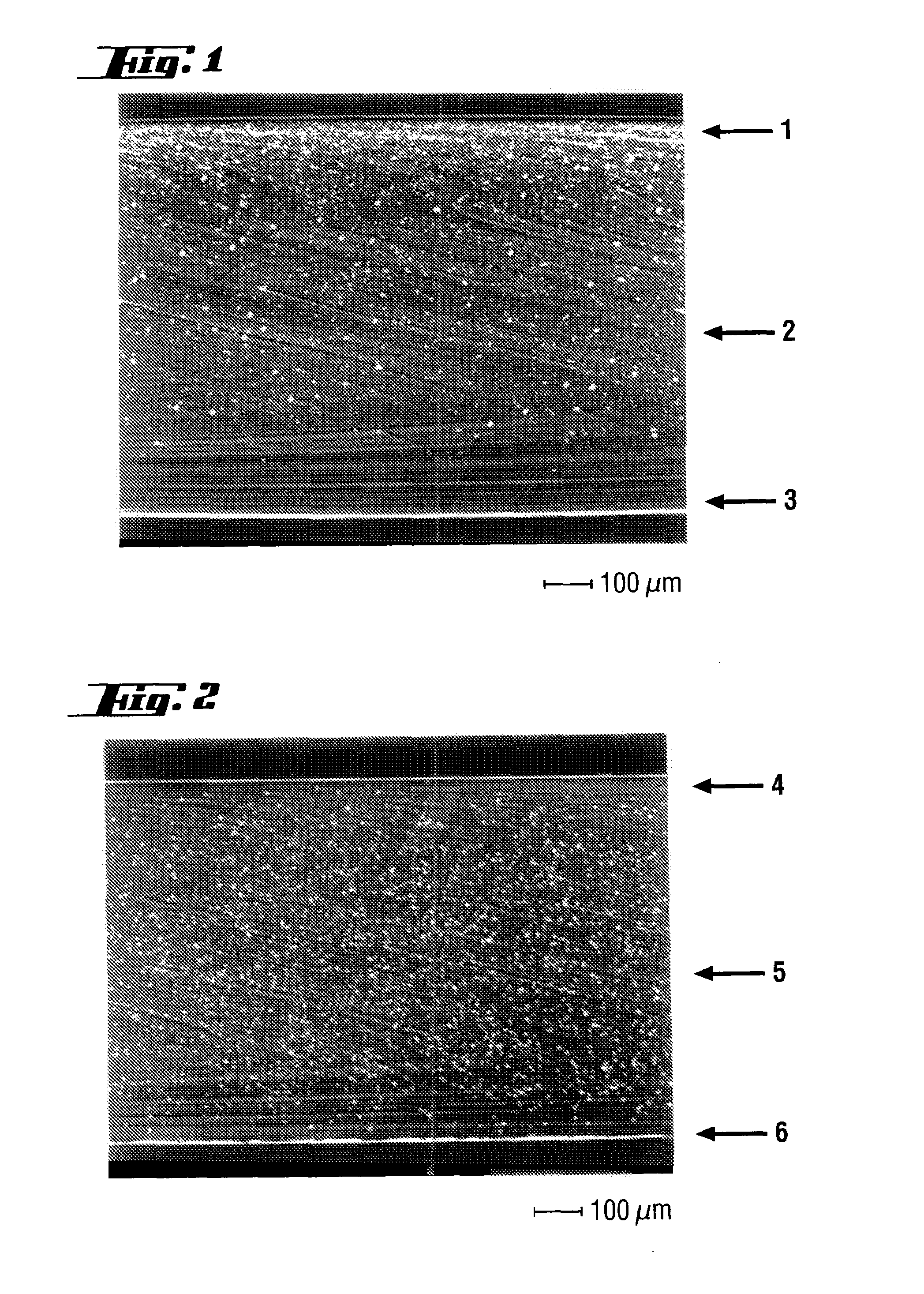
example 2a
[0044]The RTA treatment was carried out in two stages in a nitrogen atmosphere in accordance with the second process according to the invention. The RTA treatment was carried out at a heating rate of 100° C. / s to 1,200° C. The SOI wafer was then held at this temperature for 10 s and then cooled to 1,000° C. at a cooling rate of 100° C. / s. The SOI wafer was then held at 1,000° C. for 90 s before being cooled to room temperature at a cooling rate of 100° C. / s.
PUM
 Abstract
Description
Claims
Application Information