[0025]In accordance with the first aspect of the present invention, the primary molding resin is injected with the transfer material placed in the primary molding cavity, and a secondary molding cavity is formed, with a primary molded product, which is made of the primary molding resin and bonded to the transfer material, left remaining therein; therefore, it becomes possible to prevent problems such as displacement of the primary molded product. Moreover, by injecting the secondary molding resin onto the periphery of the primary molded product, the primary molded product and the secondary molded product are firmly anchored to each other so that a molded product can be manufactured. Here, the primary molded product may be formed by using a transparent primary molding resin corresponding to the transparent window section. Moreover, the primary molded product may be formed by using a resin corresponding to the main body portion. In this case, the secondary molding resin is prepared by a transparent resin corresponding to the transparent window section. With this arrangement, it is possible to manufacture a casing for an electronic apparatus in which the transparent window section and the main body portion are firmly anchored to each other.
[0026]In accordance with the fourth aspect of the present invention, the transparent window section is formed by using, as the primary molding resin, a resin that has a visible light
transmittance of 80% or more defined in JIS-K7105 and a pencil
hardness of F or more defined in JIS-K5600-5-4; thus, it is possible to manufacture the casing for an electronic apparatus that ensures the screen
visibility and scratch resistance of the transparent window section. With respect to the specific primary molding resin having these properties, for example, a resin formed by adding rubber to a
polymethyl methacrylate resin is desirably used.
[0027]In accordance with the sixth aspect of the present invention, the main body portion is formed by using, as the secondary molding resin, a resin that has an Izod impact strength of 10 KJ / m2 or more defined in ASTM-D256; thus, it is possible to manufacture a casing for an electronic apparatus that ensures sufficient strength required for the main body portion.
[0028]In accordance with the seventh aspect of the present invention, by using a resin having a molding temperature higher than that of the primary molding resin; thus, the primary molded product and the secondary molded product are firmly anchored to each other.
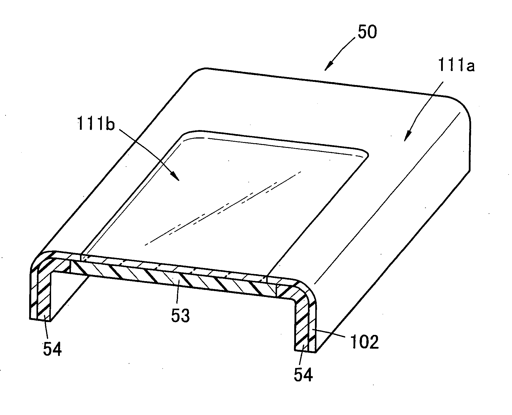
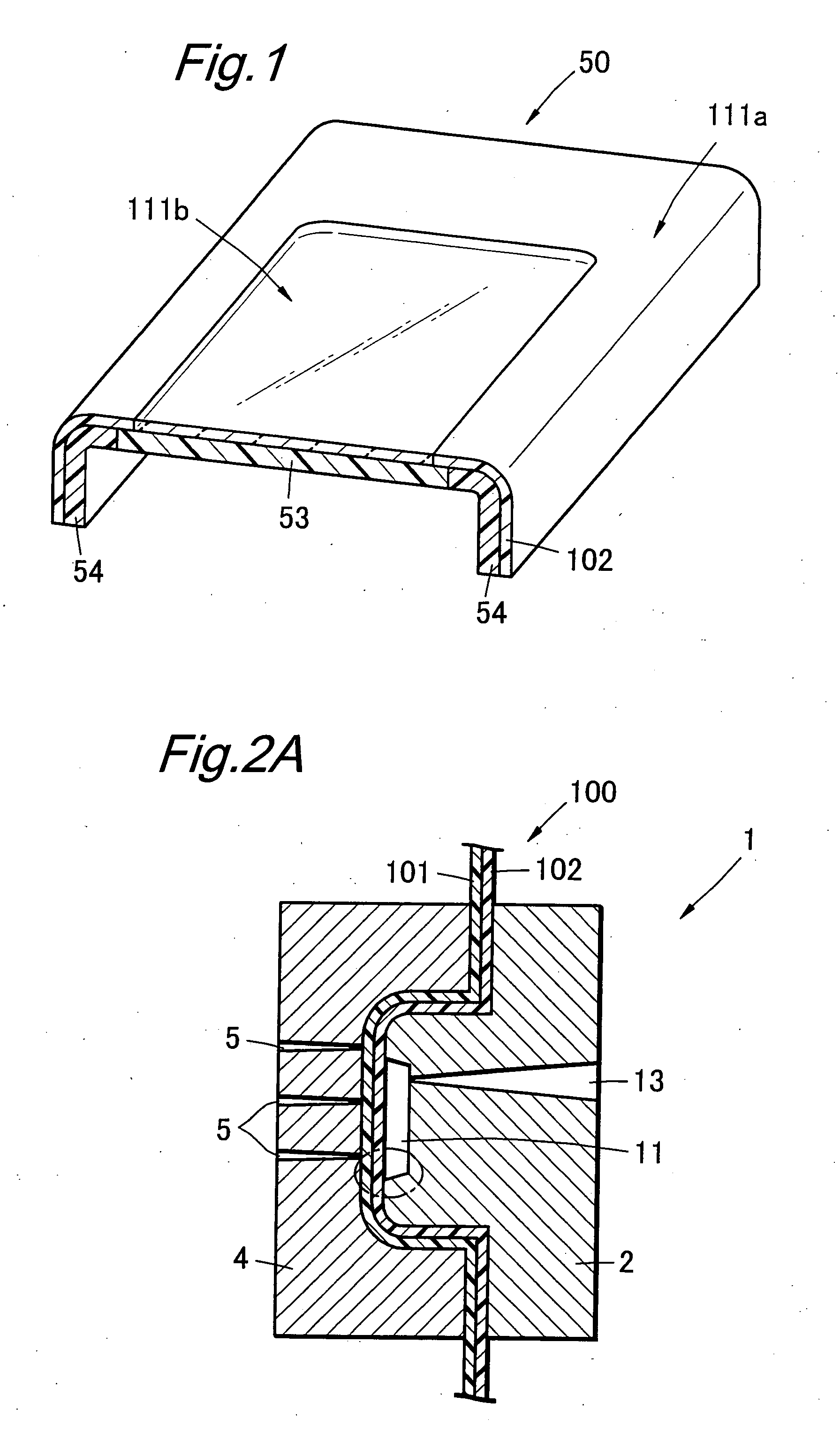
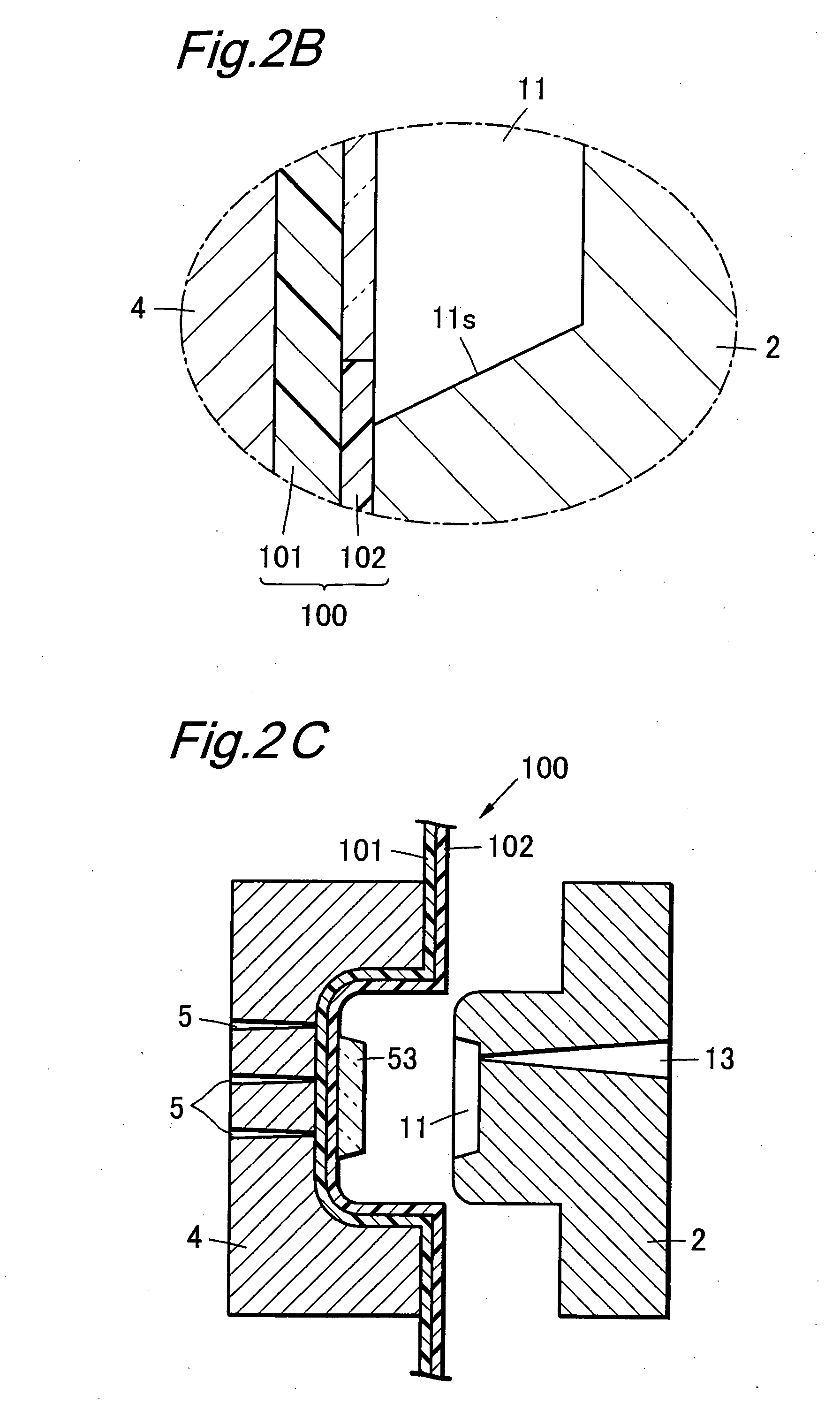
[0029]In accordance with the eighth aspect of the present invention, the transparent area of the decorative layer is made smaller than the primary molding cavity, with an opaque area formed on the periphery of the transparent area; therefore, it is possible to shield the vicinity of the anchored portion between the primary molded product and the secondary molded product.
[0030]Since the transparent area is formed by an ink containing a transparent resin, it is possible to widen an area at which the primary molded product is bonded to the decorative layer, and consequently to allow the transfer material and the primary molded product to be made in tight-contact with each other when forming the secondary molded product; thus, it becomes possible to prevent displacement and coming off of the primary molded product.BRIEF DESCRIPTIONS OF THE DRAWINGS

