Surface-conduction electron emitter and electron source using the same

a surface-conduction electron and electron source technology, applied in the field of electron emitters, can solve the problems of low brightness and narrow viewing angle when compared with the other fpds, high energy consumption, and still have problems with lcds

Active Publication Date: 2008-05-29
TSINGHUA UNIV +1
View PDF13 Cites 25 Cited by
  • Summary
  • Abstract
  • Description
  • Claims
  • Application Information

AI Technical Summary

Problems solved by technology

Among the various types of flat panel displays, liquid crystal displays are extensively investigated, but LCDs still have problems such as low brightness and narrow viewing angle when compared with the other FPDs.
For plasma display panels, high energy consumption and low color fidelity are the main obstacles.
However, the fabrication cost of the micro-tip structures is high and they are d...

Method used


Image

  • Surface-conduction electron emitter and electron source using the same
  • Surface-conduction electron emitter and electron source using the same
  • Surface-conduction electron emitter and electron source using the same

Examples


first embodiment

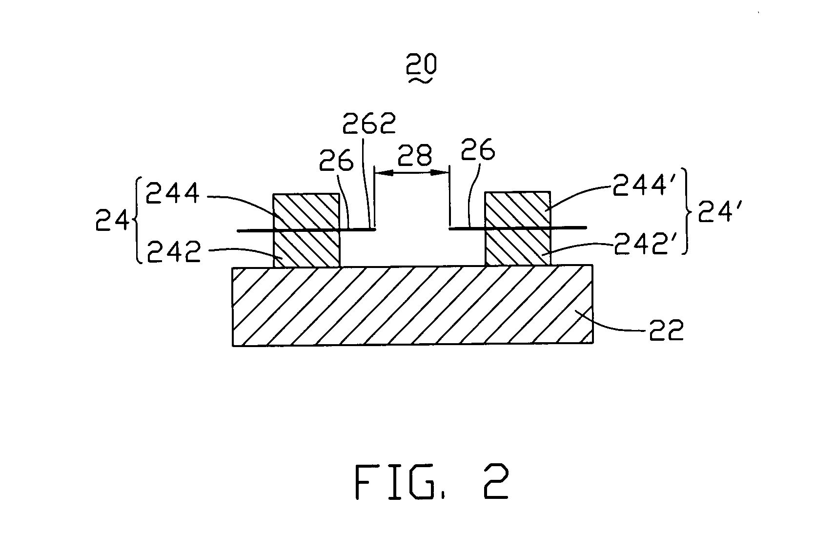
[0028]Referring to FIG. 2, a surface-conduction electron emitter 20 in the first embodiment includes a substrate 22, a first electrode 24, a second electrode 24′, and two line-shaped carbon nanotube elements 26. The first electrode 24 and the second electrode 24′ are parallel to each other and disposed on the substrate 22.

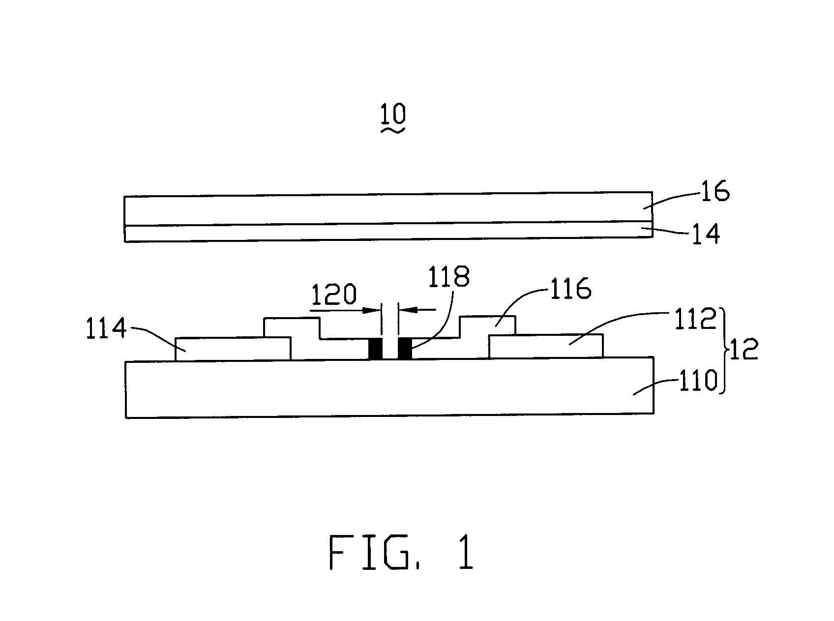
[0029]The first electrode 24 and the second electrode 24′ respectively include lower layers 242 and 242′, and upper layers 244 and 244′. The lower layers 242 and 242′ are disposed on a surface of the substrate 22. The upper layers 244 and 244′ are disposed on the lower layers 242 and 242′. Two carbon nanotube elements 26 are respectively sandwiched by the upper layers 244 and 244′ and the lower layers 242 and 242′, and thereby, fixed on the first electrode 24 and the second electrode 24′. Each carbon nanotube element 26 includes at least one emitting end 262 protruding from the first electrode 24 and / or the second electrode 24′. The emitting ends 262 of the two car...

second embodiment

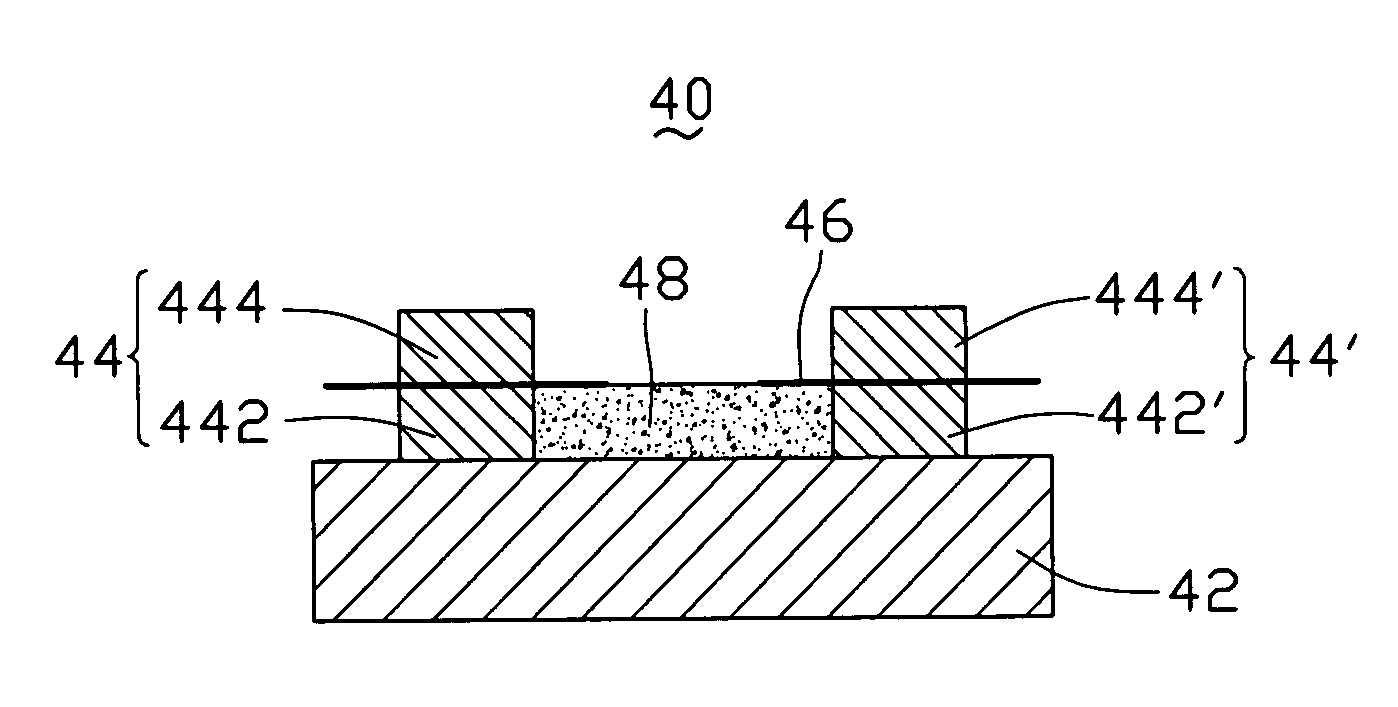
[0039]The thickness of the spacer 48 is equal to the thickness of the lower layers 442 and 442′. The spacer 48 can, beneficially, be made of a material selected from a group consisting of silicon dioxide, alumina, metal oxides, and ceramic. In the second embodiment, the spacer 48 is a layer of silicon dioxide. The thickness of the spacer 48 is in the approximate range from 40 to 70 nanometers. The spacer 48 can prevent a bend or a break of the carbon nanotube elements 40 protruding from the first electrodes 44 and the second electrodes 44′ that could be caused by effects of gravity or the electrical field.

[0040]Referring to FIG. 7, the surface-conduction electron emitter 50 in the third embodiment is similar to the surface-conduction electron emitter 20 in the first embodiment, and includes a substrate 52, a first electrode 54, a second electrode 54′, and two line-shaped carbon nanotube elements 56. The first electrode 54 and the second electrode 54′ are parallel to each other and d...


PUM


Abstract

A surface-conduction electron emitter includes a substrate, two electrodes disposed on the substrate and parallel to each other, and a plurality of line-shaped carbon nanotube elements fixed on at least one electrode. One end of each carbon nanotube element points to the other electrode. An electron source using the surface-conduction electron emitter includes a substrate, a plurality of electrodes disposed on the substrate and parallel to each other, and a plurality of line-shaped carbon nanotube elements fixed on at least one electrode. One end of each carbon nanotube element points to the other electrode.

Description

RELATED APPLICATIONS[0001]This application is related to commonly-assigned applications entitled, “METHOD FOR FABRICATING ELECTRON EMITTER”, filed _ (Atty. Docket No. US12309). Disclosure of the above-identified application is incorporated herein by reference.BACKGROUND[0002]1. Field of the Invention[0003]The invention relates generally to electron emitters and, particularly, to a surface-conduction electron emitter and an electron source using the same.[0004]2. Discussion of Related Art[0005]Recently, development of flat panel displays (FPDs) has increased. Flat panel displays include field emission displays (FED), liquid crystal displays (LCD), plasma display panels (PDP), etc.[0006]Among the various types of flat panel displays, liquid crystal displays are extensively investigated, but LCDs still have problems such as low brightness and narrow viewing angle when compared with the other FPDs. For plasma display panels, high energy consumption and low color fidelity are the main ob...

Claims


Application Information

Patent Timeline
IPC IPC(8): H01J1/88
CPCB82Y10/00H01J2201/3165H01J2201/30469H01J1/316
Inventor LIU, PENGFAN, SHOU-SHANLIU, LIANGJIANG, KAI-LI
Owner TSINGHUA UNIV
Why Eureka
Try Eureka