Methods of Forming Field Effect Transistors Having Silicon-Germanium Source and Drain Regions

a field effect transistor and silicon-germanium source technology, applied in the direction of transistors, semiconductor devices, electrical equipment, etc., can solve the problems of unstable process control of isotropic etching techniques, poor repeatability, and inability to achieve the high strain level that can be achieved

Inactive Publication Date: 2008-05-29
SAMSUNG ELECTRONICS CO LTD
View PDF26 Cites 64 Cited by
  • Summary
  • Abstract
  • Description
  • Claims
  • Application Information

AI Technical Summary

Benefits of technology

[0006]Additional embodiments of the present invention include methods of forming a field effect transistor by forming a gate electrode on a non-SiGe semiconductor substrate and then forming source and drain regions (e.g., lightly doped source and drain regions) in the substrate by selectively implanting source and drain region dopants of first conductivity type into the substrate, using the gate electrode as a first implant mask. Sidewall spacers are then formed on sidewalls of the gate electrode. The formation of the spacers is followed by a step of implanting additional source and drain region dopants into the substrate, using the gate electrode and sidewall spacers as an implant mask. The semiconductor substrate is then selectively etched to define source and drain region trenches on opposite sides of the insulated gate electrode. A native oxide material and contaminants are then removed from sidewalls of the source and drain region trenches by exposing the sidewalls of the trenches to a diluted hydrofluoric acid (HF) cleaning solution. These sidewalls are then recessed by exposing the cleaned sidewalls to another cleaning solution containing ammonium hydroxide. An epitaxial growth step is then performed to grow SiGe source and drain regions from the sidewalls of the source and drain region trenches. This epitaxial growth step may be an in-situ doped epitaxial growth step.

Problems solved by technology

Unfortunately, isotropic etching techniques may suffer from unstable process control and poor repeatability.
In contrast, anisotropic etching techniques typically provide excellent process control, but frequently do not yield the high levels of strain that can be achieved with isotropic etching techniques.

Method used


Image

  • Methods of Forming Field Effect Transistors Having Silicon-Germanium Source and Drain Regions
  • Methods of Forming Field Effect Transistors Having Silicon-Germanium Source and Drain Regions
  • Methods of Forming Field Effect Transistors Having Silicon-Germanium Source and Drain Regions

Examples


Embodiment Construction

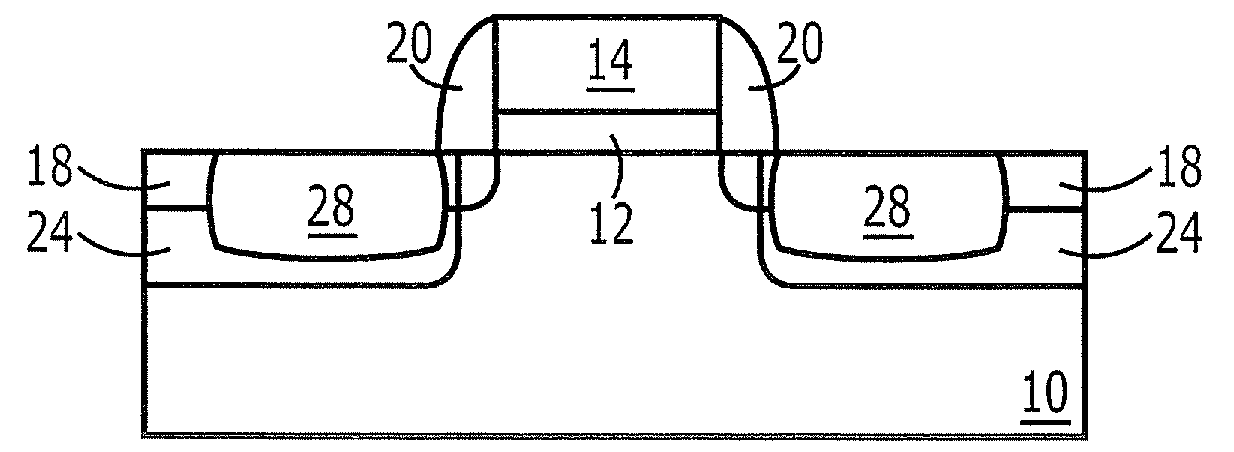
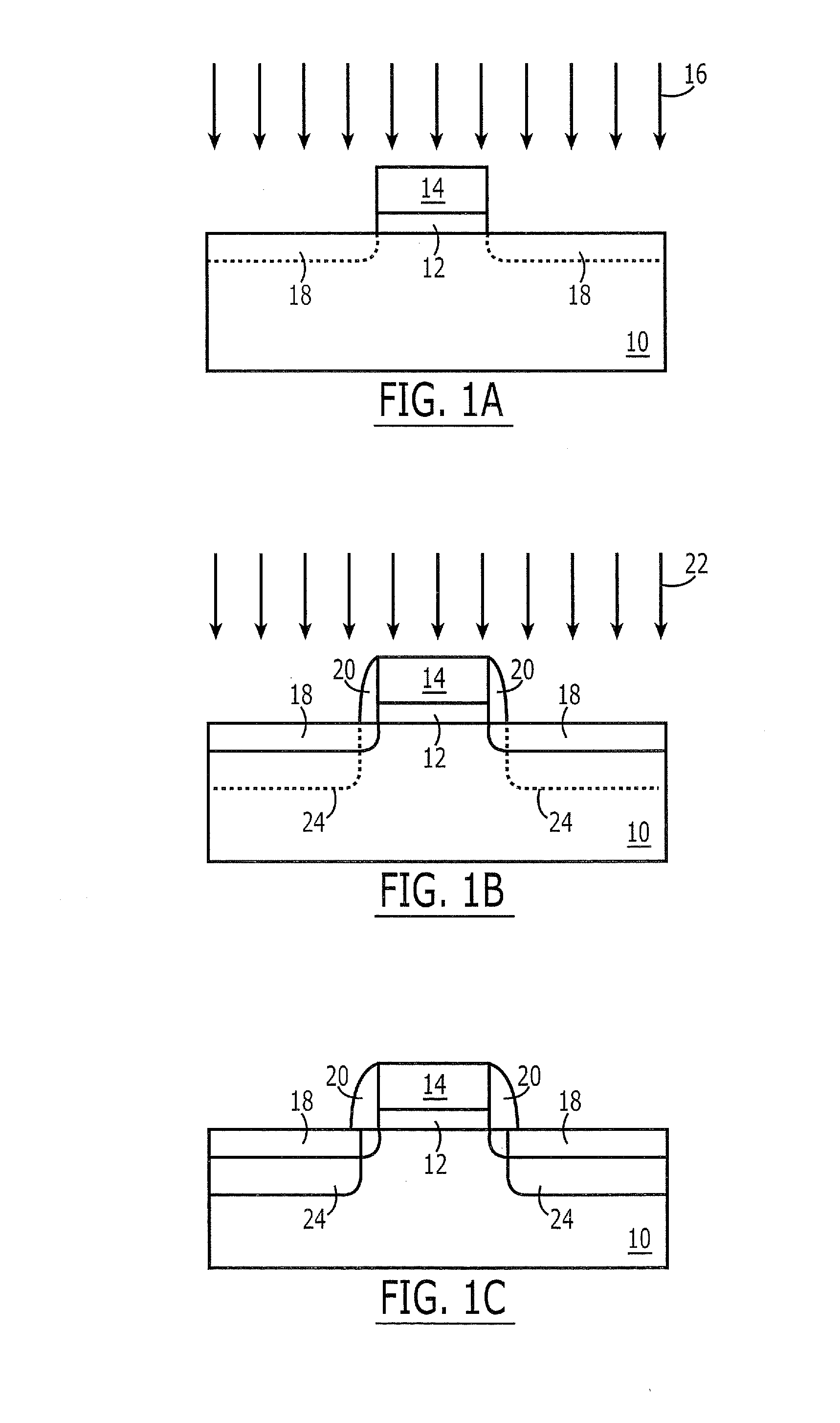
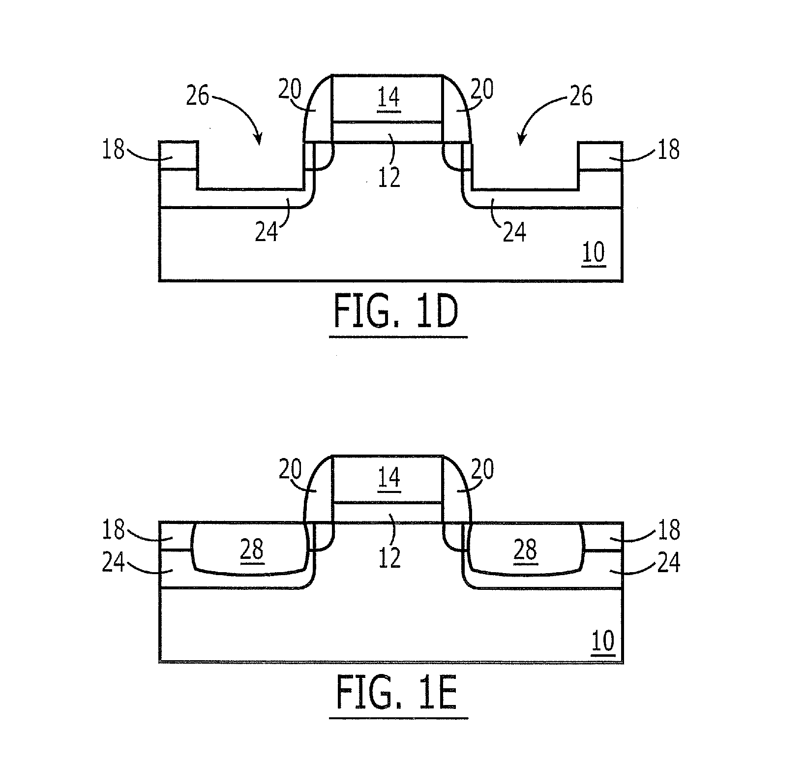
[0008]The present invention will now be described more fully hereinafter with reference to the accompanying drawings, in which preferred embodiments of the invention are shown. This invention may, however, be embodied in different forms and should not be construed as limited to the embodiments set forth herein. Rather, these embodiments are provided so that this disclosure will be thorough and complete, and will fully convey the scope of the invention to those skilled in the art. In the drawings, the thickness of layers and regions are exaggerated for clarity. It will also be understood that when a layer is referred to as being “on” another layer or substrate, it can be directly on the other layer or substrate, or intervening layers may also be present. Like numbers refer to like elements throughout.

[0009]Methods of forming field effect transistors according to some embodiments of the present invention include forming trench-based SiGe source and drain regions using a combination of...


PUM


Abstract

Methods of forming field effect transistors include forming an insulated gate electrode on a non-SiGe semiconductor substrate and then selectively etching the semiconductor substrate to define source and drain region trenches on opposite sides of the insulated gate electrode. A step is performed to remove native oxide layers from sidewalls of the source and drain region trenches. The removal of the native oxide is followed by recessing the sidewalls of the source and drain region trenches by selectively wet etching the sidewalls of the source and drain region trenches. This step of wet etching the sidewalls of the source and drain region trenches may include exposing the sidewalls to a cleaning solution including ammonium hydroxide (NH4OH). A step is then performed to epitaxially grow SiGe source and drain regions in the source and drain region trenches. This step of epitaxially growing SiGe source and drain regions may include epitaxially growing in-situ doped SiGe source and drain regions of first conductivity type in the source and drain region trenches.

Description

FIELD OF THE INVENTION[0001]The present invention relates to integrated circuit fabrication methods and, more particularly, to methods of fabricating field effect transistors in integrated circuit substrates.BACKGROUND OF THE INVENTION[0002]The electrical properties of field effect transistors may be improved by increasing the mobility of charge carriers in the channel regions of the field effect transistors. One technique to increase the mobility of charge carriers in a channel region includes adding lattice strain to the channel region. Lattice strain may be added to the channel region by generating a lattice mismatch between the channel region and source / drain regions of the field effect transistor. In some cases, a lattice mismatch may be generated by forming a heterojunction between the channel region and the source / drain regions. One technique to form a heterojunction includes forming the channel region as a silicon region and the source / drain regions as SiGe source / drain regi...

Claims


Application Information

Patent Timeline
Patent Type & Authority Applications(United States)
IPC IPC(8): H01L21/336
CPCH01L21/02057H01L29/165H01L29/7848H01L29/66636H01L29/7833H01L29/6659H01L21/18
Inventor PARK, SANG JEANYANG, JONG HO
Owner SAMSUNG ELECTRONICS CO LTD
Why Eureka
Try Eureka