High Voltage Bipolar Transistor with Pseudo Buried Layers

a high-voltage bipolar transistor and pseudo-buried layer technology, applied in the direction of transistors, semiconductor devices, electrical equipment, etc., can solve the problems of high process cost, difficult integration of high frequency and high-voltage bipolar transistors

Active Publication Date: 2011-06-16
SHANGHAI HUAHONG GRACE SEMICON MFG CORP
View PDF16 Cites 21 Cited by
  • Summary
  • Abstract
  • Description
  • Claims
  • Application Information

AI Technical Summary

Problems solved by technology

As the result, the process cost is high, also high frequency and high voltage bipolar transistors are hard to be integrated.

Method used


Image

  • High Voltage Bipolar Transistor with Pseudo Buried Layers
  • High Voltage Bipolar Transistor with Pseudo Buried Layers
  • High Voltage Bipolar Transistor with Pseudo Buried Layers

Examples


Embodiment Construction

[0004]The invention is to provide a high voltage bipolar transistor in which the breakdown voltage is increased by enlarging active critical dimension (CD) and making the depletion region of collector / base junction from 1D (vertical) distribution to 2D (vertical and lateral) distribution. The invention is low cost process.

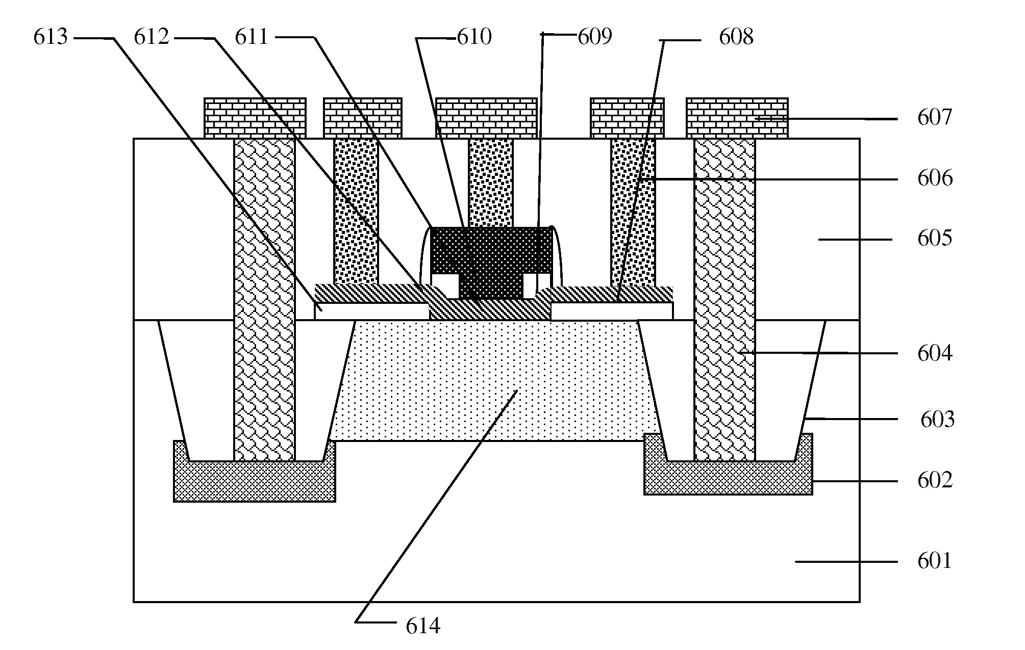
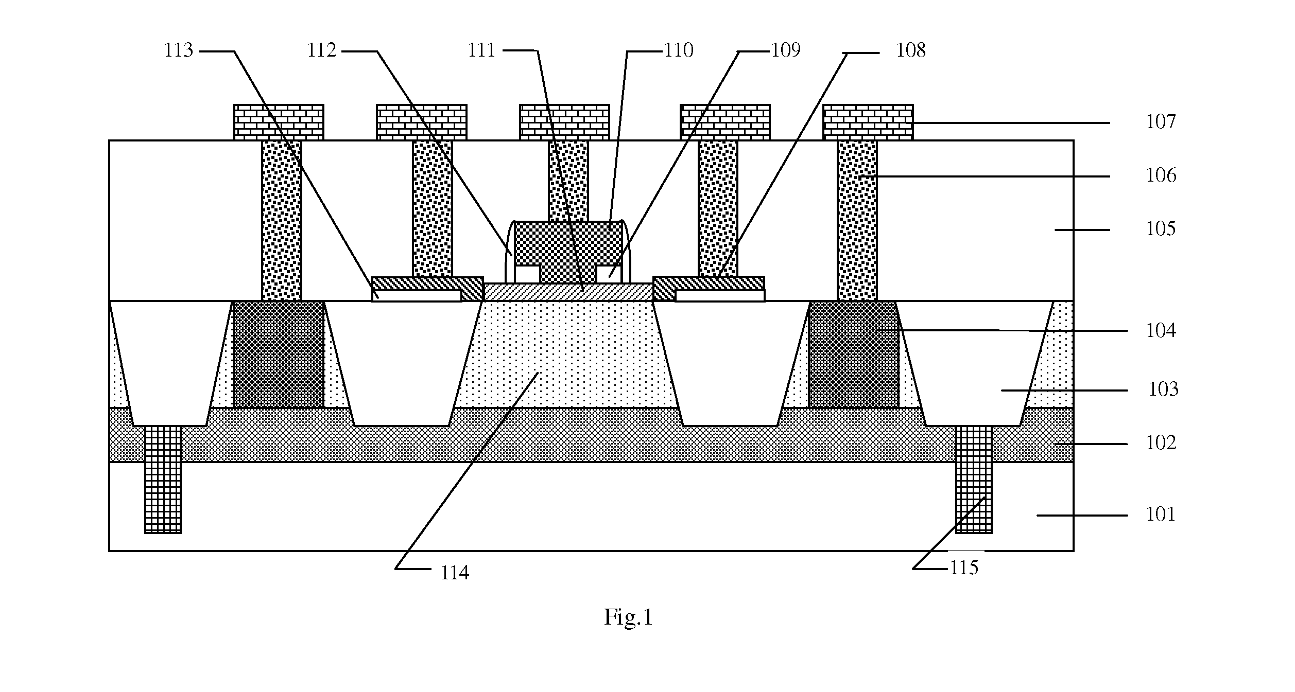
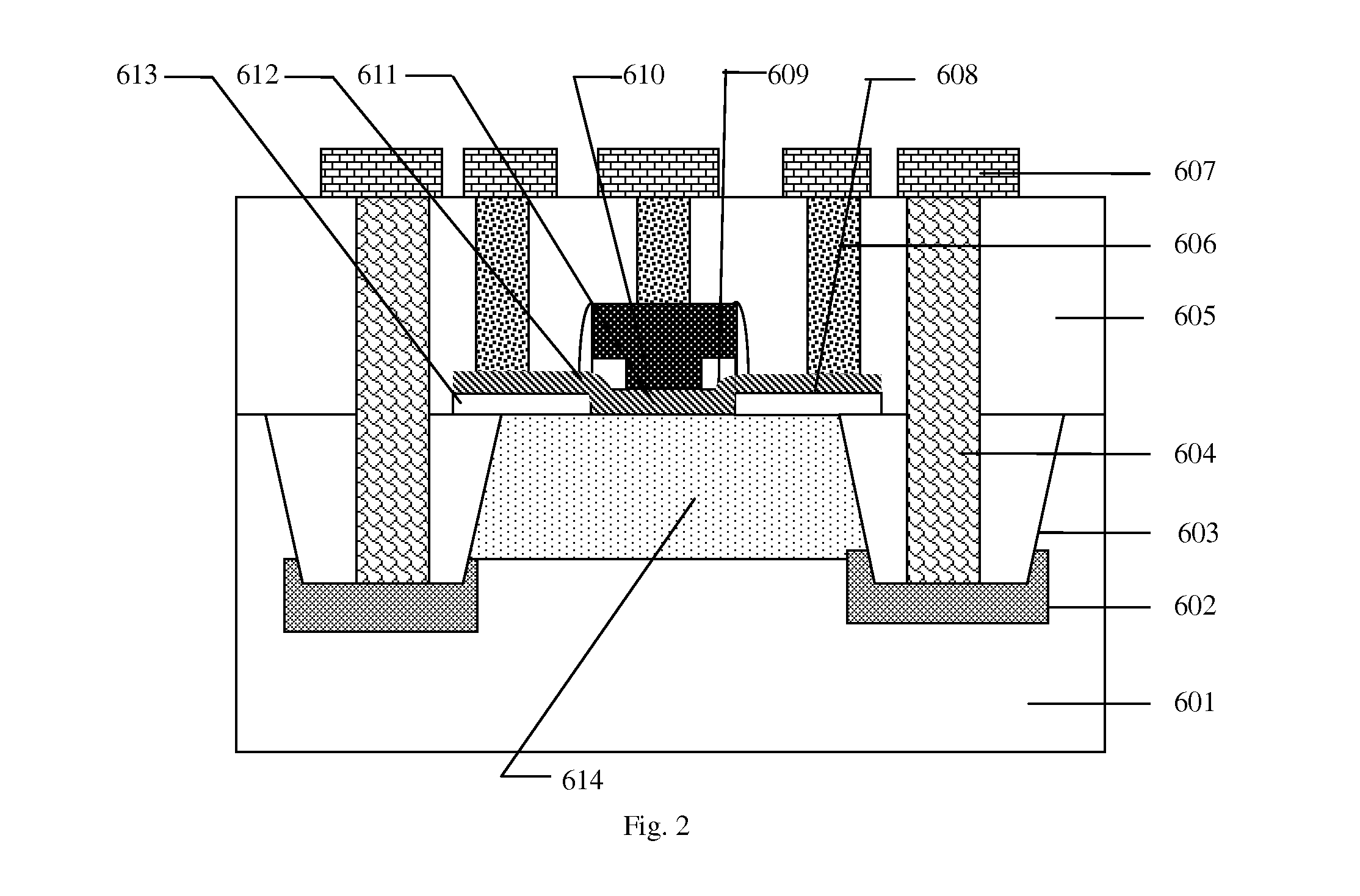
[0005]Active areas of HV bipolar transistor in this invention are isolated by shallow trench isolation (STI). The transistor comprises:

[0006]a collector, the active area with first electric type impurity doping by implants. The implants into collector can be single one or multiple steps. The implant energy is less than 50 KeV, and implant dose is less then 1e14 cm−2. The implant dose and energy can be determined by transistor breakdown voltage. Collector is connected with pseudo buried layers at two sides. Pseudo buried layers are formed by implanting high dose first type impurity through the bottoms of STI at two sides, do not touch directly and linked up by local...


PUM


Abstract

A high voltage bipolar transistor with shallow trench isolation (STI) comprises the areas of a collector formed by implanting first electric type impurities into active area and connected with pseudo buried layers at two sides; Pseudo buried layers which are formed by implanting high dose first type impurity through the bottoms of STI at two sides if active area, and do not touch directly; deep contact through field oxide to contact pseudo buried layers and pick up the collectors; a base deposited on the collector by epitaxial growth and in-situ doped by second electric type impurity, in which the intrinsic base touches local collector and extrinsic base is used for base pick-up; a emitter which is a polysilicon layer deposited on the intrinsic base and doped with first electric type impurities. This invention makes the depletion region of collector/base junction from 1D (vertical) distribution to 2D (vertical and lateral) distribution. The bipolar transistor's breakdown voltages are increased by only enlarge active critical dimension (CD). This is low-cost process.

Description

[0001]The current application claims a foreign priority to an application in China of serial number 200910201946.3 filed on Dec. 15, 2009.FIELD OF THE INVENTION[0002]This invention relates generally to semiconductor devices in integrated circuits. More particularly it relates to HV bipolar transistor design and fabrication.BACKGROUND OF THE INVENTION[0003]The background of the invention is illustrated with the example of NPN transistor. Current bipolar transistor's structure is shown as FIG. 1 including collector 114, base 111 and emitter 110. Collector 114 is N−epitaxial layer grown on N+ buried layer 102, Collector area is picked up by N-type heavy doped buried layer 102 on substrate 102, N-type high doped collector pick-up 104 in active area, deep contact 106 in interlayer dielectric (ILD) 105 and metal electrode 107. N-type high doped collector pick-up 104 is formed by high dose and high energy implant. Collector 114 is isolated by shallow trench isolation (STI) 103. Between tra...

Claims


Application Information

Patent Timeline
Patent Type & Authority Applications(United States)
IPC IPC(8): H01L29/70
CPCH01L21/76232H01L21/8249H01L27/0623H01L29/0657H01L29/7378H01L29/41708H01L29/66242H01L29/66287H01L29/7322H01L29/0821
Inventor CHIU, TZUYINCHU, TUNGYUANQIAN, WENSHENGFAN, YUNGCHIEHHU, JUNLIU, DONGHUALV, YUKUN
Owner SHANGHAI HUAHONG GRACE SEMICON MFG CORP
Why Eureka
Try Eureka