Manufacturing Method of a Semiconductor Device, and Substrate Processing Apparatus

a manufacturing method and semiconductor technology, applied in semiconductor/solid-state device manufacturing, electrical equipment, basic electric elements, etc., can solve problems such as increasing wiring resistan

Active Publication Date: 2008-05-29
KOKUSA ELECTRIC CO LTD
View PDF3 Cites 14 Cited by
  • Summary
  • Abstract
  • Description
  • Claims
  • Application Information

AI Technical Summary

Benefits of technology

[0014]In the first aspect of the present invention, a hydrogen-containing gas is introduced in advance of an oxygen-containing gas; accordingly, initial-stage oxidation of the substrate surface prior to the regular oxidation can be suppressed, and the natural oxidation film on the surface of the substrate can be removed.
[0015]Furthermore, in cases in which at least a layer that contains silicon atoms but does not contain metal atoms and a layer that contains metal atoms are exposed at the surface of the substrate in accordance with the other aspect of the present invention, only the layer that contains silicon atoms but does not contain metal atoms can be selectively oxidized without oxidizing the layer that contains metal atoms.

Problems solved by technology

As the degree of integration of semiconductor devices has increased, an increase in wiring resistance has become a problem.

Method used


Image

  • Manufacturing Method of a Semiconductor Device, and Substrate Processing Apparatus
  • Manufacturing Method of a Semiconductor Device, and Substrate Processing Apparatus
  • Manufacturing Method of a Semiconductor Device, and Substrate Processing Apparatus

Examples


Embodiment Construction

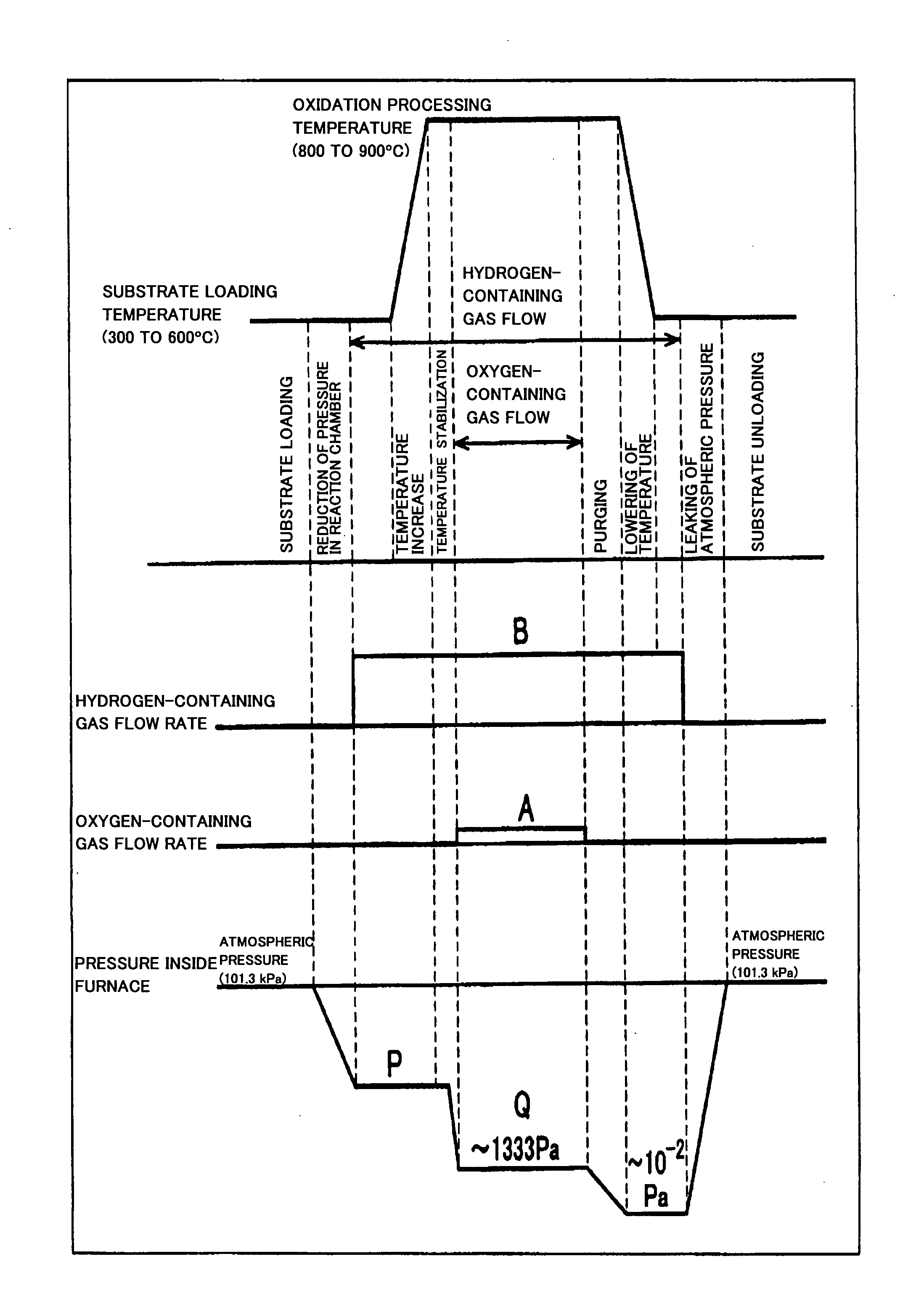
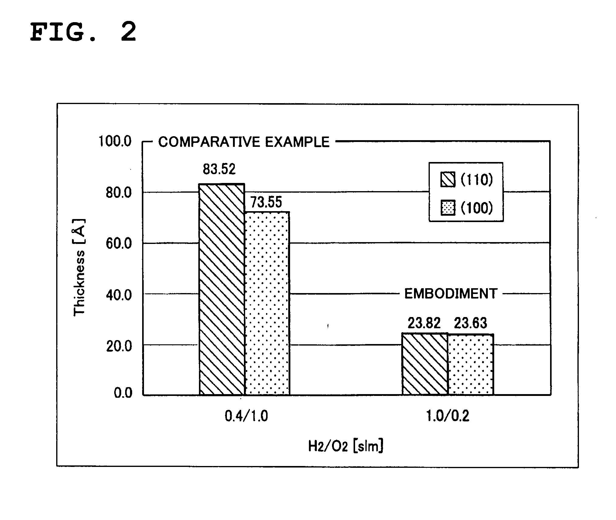
[0016]The present inventors discovered that even if the hydrogen-containing gas is introduced into the processing chamber in advance of the oxygen-containing gas, no localized volume expansion occurs in the processing chamber as long as the interior of the processing chamber is placed under a reduced pressure. Furthermore, the present inventors discovered that the oxidation reaction of the silicide film or metal material (layer that contains metal atoms) exposed at the surface can be suppressed by placing the interior of the processing chamber under a reduced pressure and introducing the hydrogen-containing gas in advance of the oxygen-containing gas into the processing chamber after the substrate is loaded into the processing chamber. Moreover, the present inventor discovered that the natural oxidation film that is formed on a surface of the substrate can also be removed in this case. In addition, the present inventor discovered conditions under which the recovery from damage to th...


PUM

PropertyMeasurementUnit
pressureaaaaaaaaaa
temperatureaaaaaaaaaa

Abstract

An object of this invention is to make it possible to suppress early-stage oxidation of a substrate surface prior to oxidation processing, and to remove a natural oxidation film. For this reason, a method is provided comprising the steps of loading a substrate into a processing chamber, supplying a hydrogen-containing gas and an oxygen-containing gas into the processing chamber, and subjecting a surface of the substrate to oxidation processing, and unloading the substrate subjected to oxidation processing from the processing chamber. In the oxidation processing step, the hydrogen-containing gas is introduced in advance into the processing chamber, with the pressure inside the processing chamber set at a pressure that is less than atmospheric pressure, and the oxygen-containing gas is then introduced in the state in which the introduction of the hydrogen-containing gas is continued.

Description

TECHNICAL FIELD[0001]The present invention relates to a manufacturing method of a semiconductor device and to a substrate processing apparatus for the oxidation processing of a substrate surface.BACKGROUND ART[0002]As the degree of integration of semiconductor devices has increased, an increase in wiring resistance has become a problem. The materials of gate electrodes primarily used in memory processes have shifted from conventional polysilicon doped with impurities to silicide films that make it possible to lower the resistance value and polymetal structures in which metal materials such as tungsten and the like are stacked on top of polysilicon. Here, silicide films (also referred to as silicate films) are films that are formed by the fusion of metals and silicon. Polymetal structures are structures in which metals are stacked on top of polysilicon, and are structures in which a barrier metal is inserted between the polysilicon and metal in order to prevent silicate formation.[00...

Claims


Application Information

Patent Timeline
Patent Type & Authority Applications(United States)
IPC IPC(8): H01L21/31H01L21/306
CPCH01L21/0223H01L21/31662H01L21/02255H01L21/02238H01L21/20H01L21/205
Inventor YUASA, KAZUHIROMEGAWA, YASUHIRO
Owner KOKUSA ELECTRIC CO LTD
Why Eureka
Try Eureka