Semiconductor Device and Manufacturing Method Thereof
a semiconductor and semiconductor technology, applied in the direction of transistors, solid-state devices, transportation and packaging, etc., can solve the problems of reducing yield, deteriorating operating characteristics of thin-film transistors, and reducing reliability, so as to reduce adverse effects on semiconductor devices due to characteristics of the end portion of the semiconductor layer, reduce defects, and improve reliability
- Summary
- Abstract
- Description
- Claims
- Application Information
AI Technical Summary
Benefits of technology
Problems solved by technology
Method used
Image
Examples
embodiment mode 1
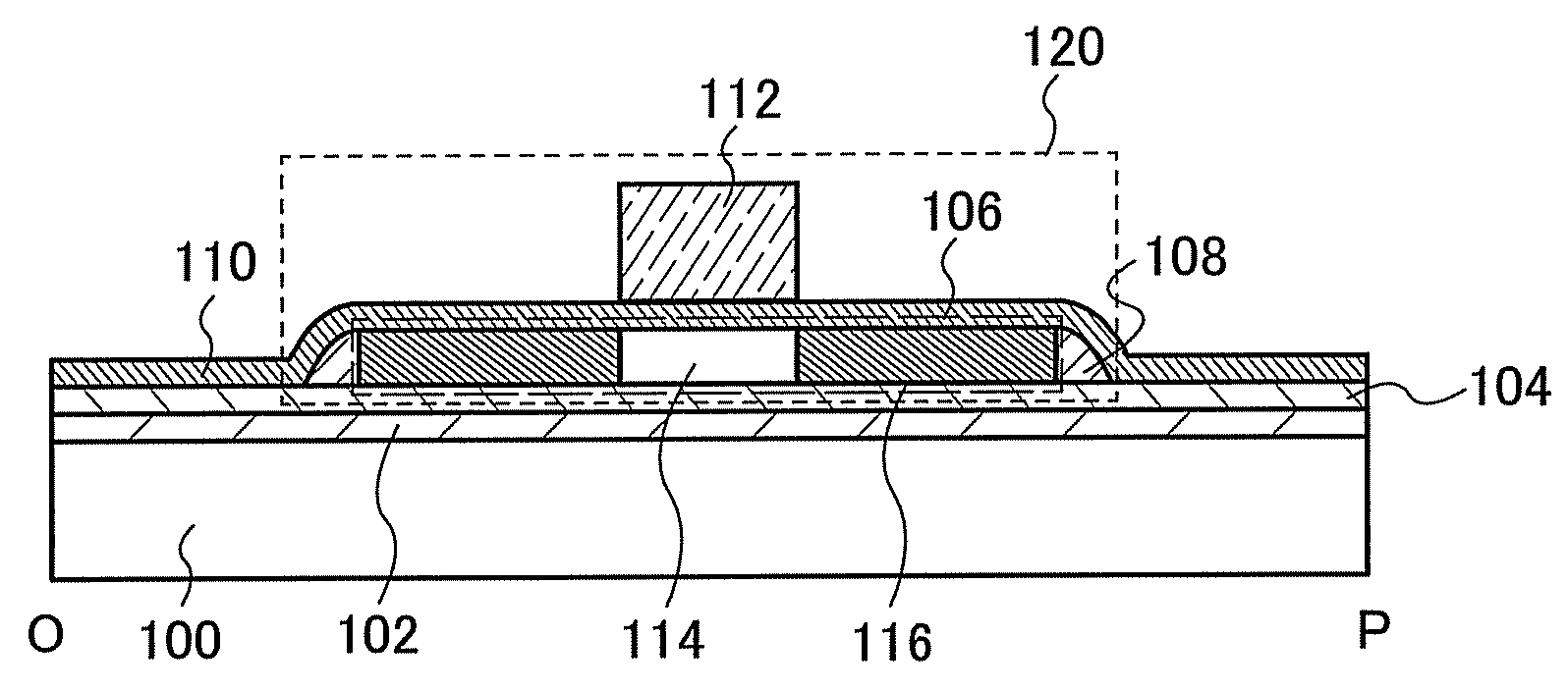
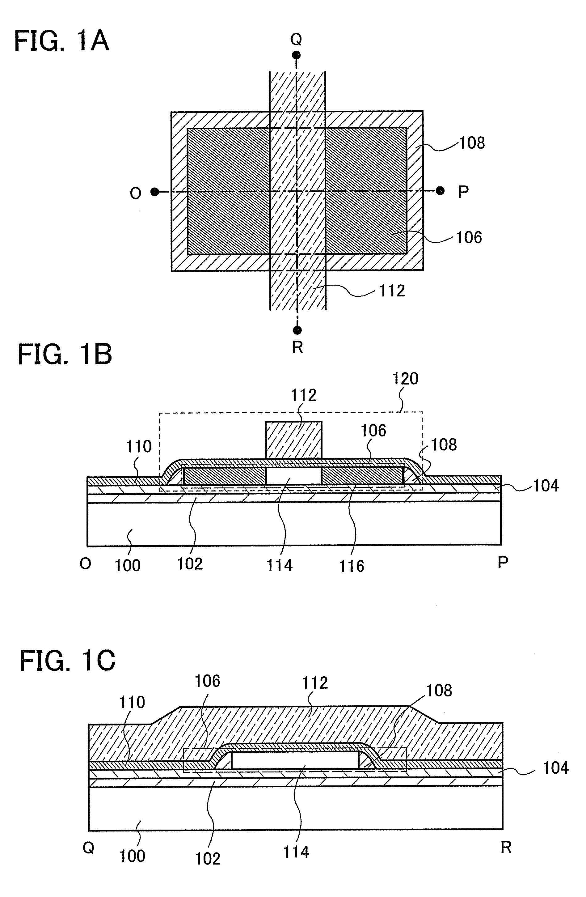
[0058]FIG. 1A is a top diagram and FIGS. 1B and 1C are cross-sectional diagrams for describing a main structure of a semiconductor device of the present invention. FIGS. 1A to 1C particularly show a structure of a thin film transistor; FIG. 1A is a top diagram, FIG. 1B is a cross-sectional diagram along a dashed line O-P in FIG. 1A, and FIG. 1C is a cross-sectional diagram along a dashed line Q-R in FIG. 1A. Note that a thin film and the like are partially omitted in FIG. 1A.
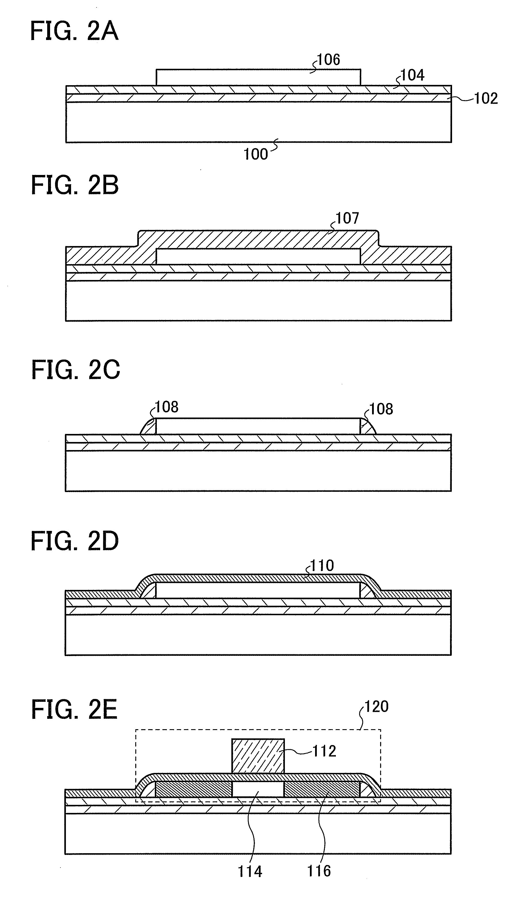
[0059]A thin film transistor 120 shown in FIG. 1A is provided over a substrate 100 having an insulating surface. The thin film transistor 120 includes a semiconductor layer 106, an insulating layer 108 which is provided so as to be in contact with a side surface of the semiconductor layer 106, an insulating layer 110 which is provided over one surface of the semiconductor layer 106, and a conductive layer 112 which is provided over the semiconductor layer 106 with the insulating layer 110 interposed therebetween...
embodiment mode 2
[0110]In this embodiment mode, an example of manufacturing a semiconductor device by a manufacturing method which is different from that in Embodiment Mode 1 is described with reference to FIGS. 3A to 3E.
[0111]First, a first semiconductor layer 306 is formed over a substrate 300, with an insulating layer 302 and an insulating layer 304 that function as a base insulating layer interposed therebetween (see FIG. 3A). Next, a first insulating layer 308 is formed to cover the first semiconductor layer 306 (see FIG. 3B). Note that up to and including the formation of the first insulating layer 308, the description made on the substrate 100, the insulating layer 102, the insulating layer 104, the semiconductor layer 106, and the first insulating layer 107 in Embodiment Mode 1 can be referred to, and therefore, a rough description thereof is made below.
[0112]As the substrate 300, a substrate having an insulating surface such as a glass substrate or a quartz substrate can be used. Each of th...
embodiment mode 3
[0146]In this embodiment mode, an example of manufacturing a semiconductor device by a manufacturing method that is different from that of foregoing Embodiment Mode 1 is described with reference to FIGS. 5A to 5E.
[0147]First, a first semiconductor layer 406 is formed over a substrate 400 with an insulating layer 402 and an insulating layer 404 that function as a base insulating layer interposed therebetween (see FIG. 5A). Next, a first insulating layer 408 is formed to cover the first semiconductor layer 406 (see FIG. 5B). Up to and including the formation of the first insulating layer 408, the description made on the substrate 100, the insulating layer 102, the insulating layer 104, the semiconductor layer 106, and the insulating layer 107 in Embodiment Mode 1 can be referred to, and therefore, the description thereof is roughly made below.
[0148]As the substrate 400, a substrate having an insulating surface such as a glass substrate or a quartz substrate can be used. Each of the in...
PUM
 Abstract
Description
Claims
Application Information


