Junction isolated poly-silicon gate JFET

a polysilicon gate and junction isolation technology, applied in the field of junction isolation polysilicon gate jfet, can solve problems such as inoperative rendering

Inactive Publication Date: 2008-06-05
DSM SOLUTIONS
View PDF18 Cites 23 Cited by
  • Summary
  • Abstract
  • Description
  • Claims
  • Application Information

AI Technical Summary

Benefits of technology

[0031]The teachings of the invention contemplate a method and device structure to build a Junction Field Effect Transistor using junction isolation only, with no Shallow Trench Isolation (STI), and a novel method of forming the active area and a novel way of forming the source, drain and gate regions and interconnects bet

Problems solved by technology

Since the source- and drain- and gate-contact poly-silicon or metal interconnect “wires” all run across what used to be the STI insulation field, the electrical contact between these “wire

Method used


Image

  • Junction isolated poly-silicon gate JFET
  • Junction isolated poly-silicon gate JFET
  • Junction isolated poly-silicon gate JFET

Examples


embodiment

Preferred Embodiment

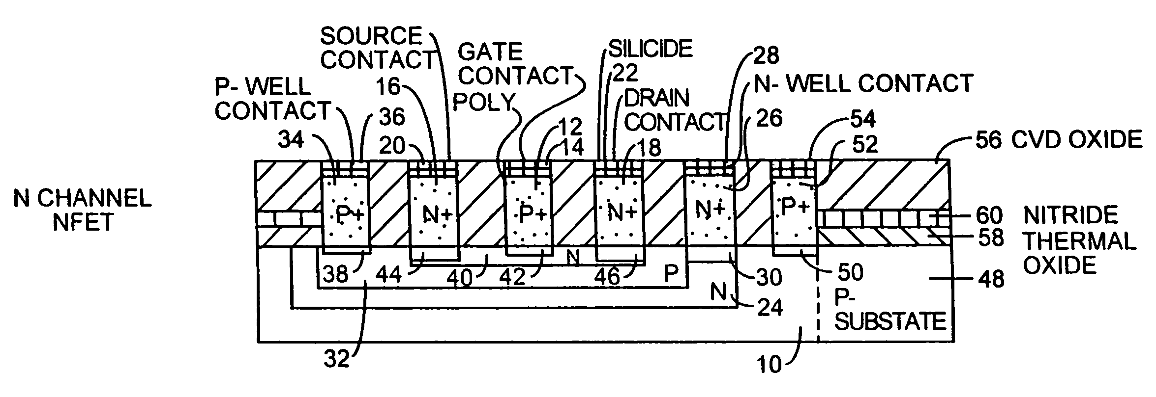
[0036]FIG. 8 is comprised of FIGS. 8A through 8D, and shows the details of the finished device. FIG. 8A is a cross-section through the finished device active area, less contact holes and metallization, and is section AA′ in FIG. 8D. FIG. 8B is a cross-section through the finished device at the gate (section BB′ in FIG. 8D). FIG. 8C is a cross-section through the finished device at the source (Section CC′ in FIG. 8D). FIG. 8D is a top view of the finished device looking down on the active area (silicide on top of the poly-silicon contacts is not shown). The finished device structure will be discussed with reference to all of FIGS. 8A through 8D. Dashed line 10 in FIG. 8D is the outline of the active area. A region of P+ doped poly-silicon 12 is the gate contact. The gate contact poly-silicon has silicide 14 formed on top thereof to reduce its resistance and to short out any PN junctions which are inadvertently formed if the gate poly-silicon 12 is extended to make...


PUM


Abstract

An integrated Junction Field Effect Transistor is disclosed which is much smaller and much less expensive to fabricate because it does not use Shallow Trench Isolation or field oxide in the semiconductor substrate to isolate separate transistors. Instead, a layer of insulating material is formed on the top surface of said substrate, and interconnect trenches are etched in said insulating layer which do not go all the way down to the semiconductor substrate. Contact openings are etched in the insulating layer all the way down to the semiconductor layer. Doped poly-silicon is formed in the contact openings and interconnect trenches and silicide is formed on tops of the poly-silicon. This contact and interconnect structure applies to any integrated transistor. The integrated JFET disclosed herein does not use STI or field oxide and uses junction isolation. A conventional JFET is built in a P-well. The P-well is encapsulated in an N-well which is implanted into the substrate. Separate contacts to the P-well, N-well and substrate are formed as well as to the source, drain and gate so that the device can be isolated by reverse-biasing a PN junction. Operating voltage is restricted to less than 0.7 volts to prevent latching.

Description

BACKGROUND OF THE INVENTION[0001]In the early day of bipolar transistor integration, aluminum contact wires were used. They ran across fields of silicon dioxide which were deposited on the surface of the substrate and then dipped down into contact holes for emitter, base and collector. Since the silicon dioxide layer was about 5000 angstroms thick, step coverage was a problem because the aluminum often would break down at the step and cause an open circuit. Isolation between active areas was accomplished using diffused PN junctions. Basically, P-type isolation diffusions were made into N-epitaxial layers to create PN junctions at the walls of the active areas between the P-type diffusion and the N-type epitaxial silicon. This created N-type islands of N-epitaxial silicon which were isolated from the substrate and each other by reverse-biased diodes. Hamilton and Howard, Basic Integrated Circuit Engineering, FIG. 1-6, p. 13 (McGraw Hill 1975), the entirety of which is hereby incorpor...

Claims


Application Information

Patent Timeline
IPC IPC(8): H01L29/76H01L21/337
CPCH01L27/098H01L29/808H01L29/66901
Inventor VORA, MADHUKAR B.
Owner DSM SOLUTIONS
Why Eureka
Try Eureka