

Structure and method for multiple height finfet devices
a technology of finfets and structures, applied in the direction of semiconductor devices, basic electric elements, electrical apparatus, etc., can solve the problems of unique design challenges, the on-current may not be increased by an arbitrary numerical factor, and the on-current may not achieve such scalability, so as to enhance the scalability of the on-current of the finfets
- Summary
- Abstract
- Description
- Claims
- Application Information
AI Technical Summary
Benefits of technology
Problems solved by technology
Method used
Image

Examples
second embodiment
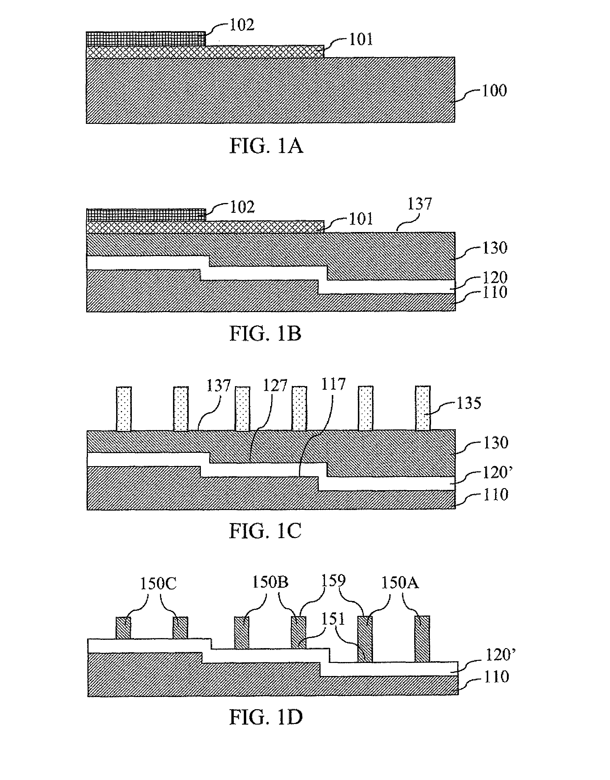
[0047]Thereafter, formation of a gate dielectric and a gate electrode follows. This part will be described below after describing the distinct parts of the present invention.
[0048]According to the second embodiment of the present invention, the same initial semiconductor substrate 100 (without the oxygen implant mask layers 101, 102) as in the first embodiment of the present invention as shown in FIG. 1A is provided first. Multiple rounds of oxygen implantation are performed. Each round of oxygen implantation is performed with only one oxygen implantation mask layer or with no oxygen implantation mask layer.
first embodiment
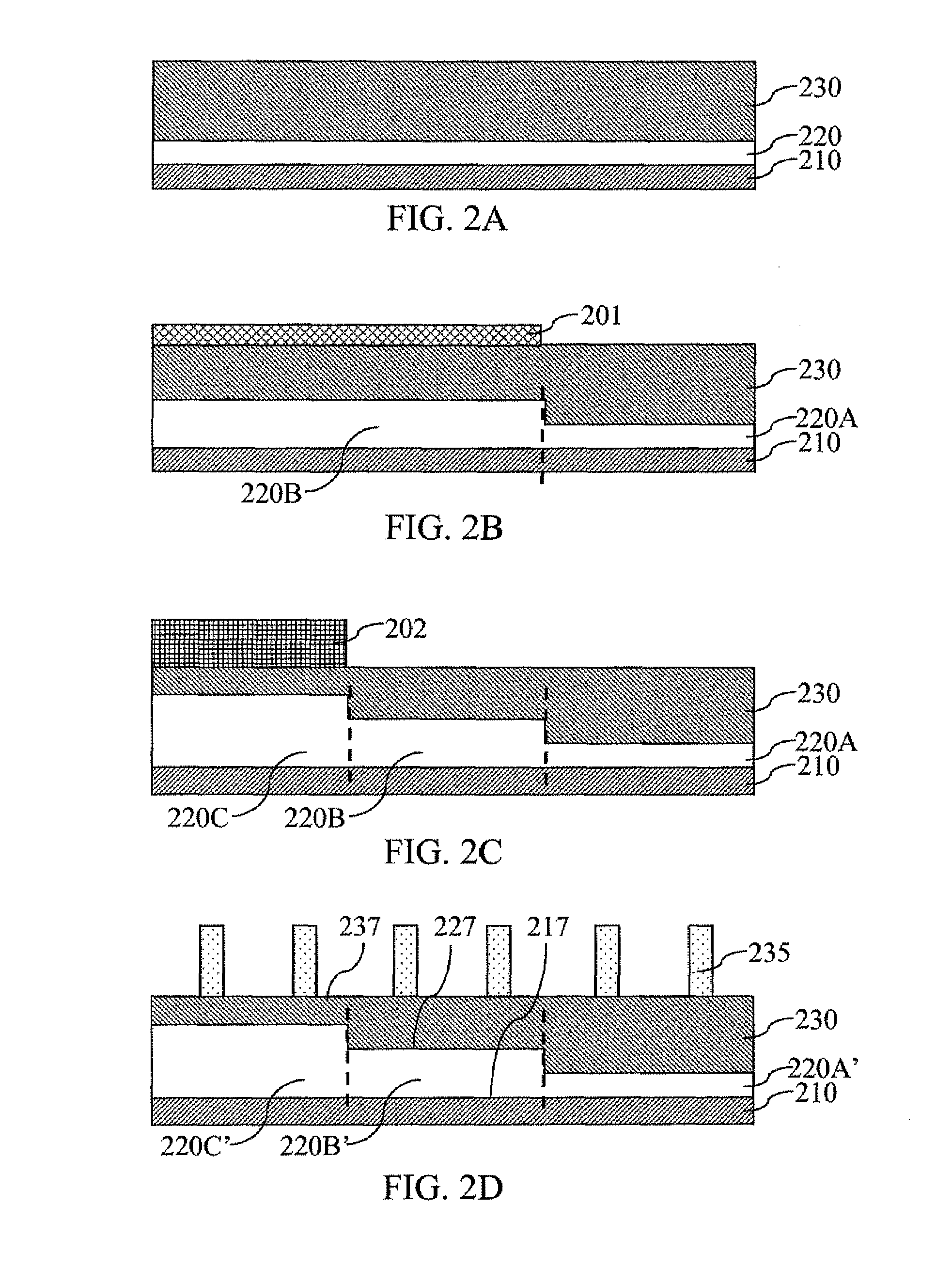
[0049]In the exemplary sequence shown in the figures, the initial semiconductor substrate 100 is implanted with oxygen to form an oxygen rich layer 220 as shown in FIG. 2A. In a manner similar to the present invention, a semiconductor substrate 210 and the top semiconductor layer 230 are also formed.
[0050]A first oxygen implant mask layer 201 is deposited and patterned according to the second embodiment of the present invention. As in the first embodiment of the present invention, any of oxygen implant mask layers, including the first oxygen implant mask layer 201, may be either a hardmask or a softmask. Oxygen is thereafter implanted into the top semiconductor layer 230 to thicken a second portion of the existing oxygen rich layer 220 under the first oxygen implant mask layer 201. In the resulting structure, the oxygen rich layer 220 has two portions: a first portion 220A of the oxygen rich layer 220 that has the original thickness as in FIG. 2A and the second portion 220B of the o...
third embodiment
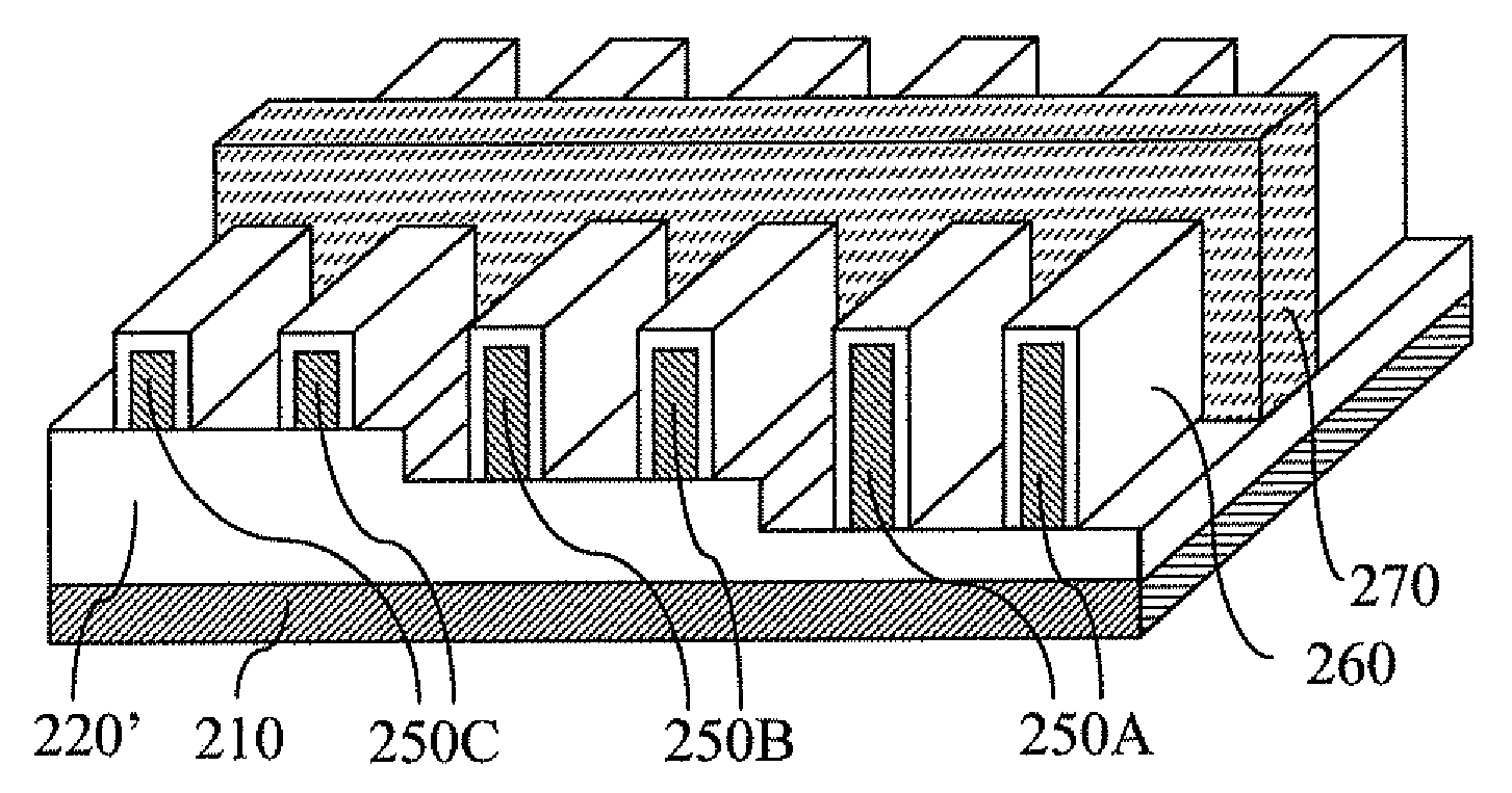
[0064]In a different perspective, the structures according to the present invention is obtained by not stopping the etch of the top semiconductor layer (130 or 230) at the oxide top surface (127 or 227) with a selective etch but instead continuing the etch into at least a portion of the buried oxide layer 320 (equivalent to 120′ or 220′) with a non-selective etch. The apparent inclusion of the lower oxide portion into the fins thus obtained is an unavoidable consequence of such an etch process.
[0065]The resulting structure has at least two upper semiconductor portions (352A-C) that have different vertical lengths, that is, different distances between the top surface of the upper semiconductor portion, which is the fin top surface 359, and the bottom surface of the upper semiconductor portion, also called “upper semiconductor portion bottom surface”351. The bottom of the fins maybe the bottom surface of the lower oxide portion (322B, 322C) if a lower oxide portion (322B, 322C) is par...
PUM
 Abstract
Description
Claims
Application Information