Plasma display panel and field emission display

a display panel and field emission technology, applied in the field of plasma display panel and field emission display, can solve the problems of insufficient anti-reflection function of cone-shaped or pyramid-shaped anti-reflection structure, difficult to perform anti-reflection treatment of all incident lights from external, etc., to achieve high anti-reflection function, diffuse light, and increase the amount of incident light from external entering the pyramidal projection of the anti-reflection layer

Active Publication Date: 2008-06-05
SEMICON ENERGY LAB CO LTD
View PDF99 Cites 38 Cited by
  • Summary
  • Abstract
  • Description
  • Claims
  • Application Information

AI Technical Summary

Benefits of technology

[0018]The PDP and the FED of the present invention are each provided with an anti-reflection layer having a plurality of pyramidal projections arranged without any spaces on a surface. Since a side surface of a pyramidal projection is not parallel to a display screen, incident light from external is not reflected to a viewer side but is reflected to another adjacent pyramidal projection or travels among the pyramidal projections. In addition, hexagonal pyramidal projections have a close-packed structure without any spaces and have an optimal shape having the largest number of side surfaces of a pyramidal projection among such shapes and a high anti-reflection function that can diffuse light in many directions efficiently. One part of incident light enters pyramidal projections, and the other part of the incident light is then incident on an adjacent pyramidal projection as reflected light. In this manner, incident light from external reflected at the surface of the side of a pyramidal projection is repeatedly incident on adjacent pyramidal projections.
[0019]In other words, of the incident light from external that is incident on the anti-reflection layer, the number of times that the light is incident on the pyramidal projections of the anti-reflection layer is increased; therefore, the amount of incident light from external entering the pyramidal projection of the anti-reflection layer is increased. Thus, the amount of incident light from external reflected to a viewer side can be reduced, and the cause of reduction in visibility such as reflection can be prevented.
[0020]Furthermore, since the protective layer is formed in the space among the pyramidal projections in the present invention, the entry of a contaminant such as dust into the space among the pyramidal projections can be prevented. Therefore, a decrease in an anti-reflection function due to the entry of dust or the like can be prevented, and physical strength of the PDP and the FED can be increased by filling the space among the pyramidal projections. Accordingly, reliability can be improved.
[0021]Accordingly, a PDP and an FED that each have higher quality and higher performance can be manufactured.

Problems solved by technology

However, with the above-described multilayer structure, lights which cannot be cancelled in the lights from external reflected at interfaces are emitted to the viewer side as reflected light.
In order to achieve mutual cancellation of incident lights from external, it has been necessary to precisely control optical characteristics of materials, thicknesses, and the like of films stacked, and it has been difficult to perform anti-reflection treatment for all incident lights from external which are incident from various angles.
In addition, a cone-shaped or pyramid-shaped anti-reflection structure has not had a sufficient anti-reflection function.

Method used


Image

  • Plasma display panel and field emission display
  • Plasma display panel and field emission display
  • Plasma display panel and field emission display

Examples


embodiment mode 1

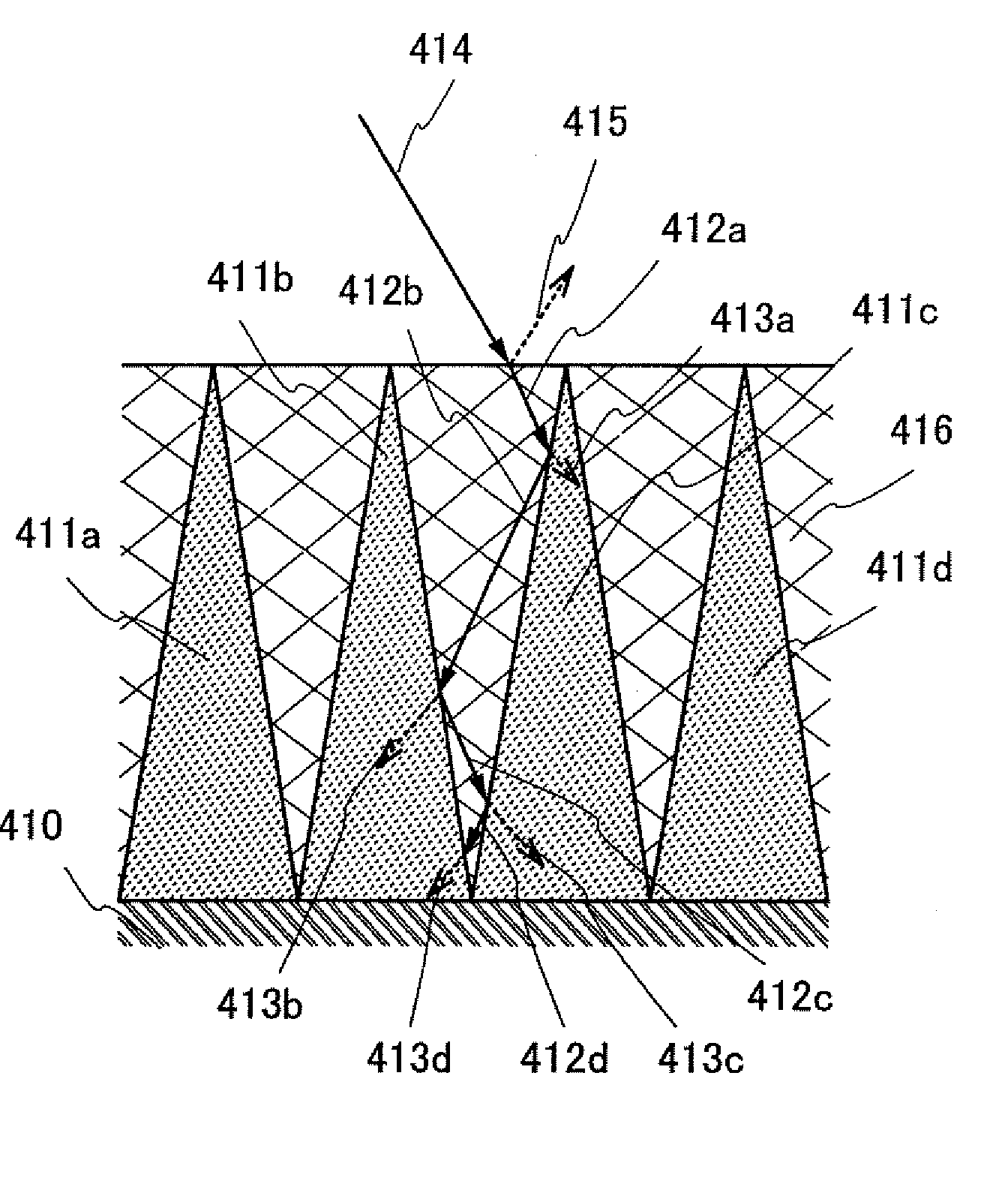
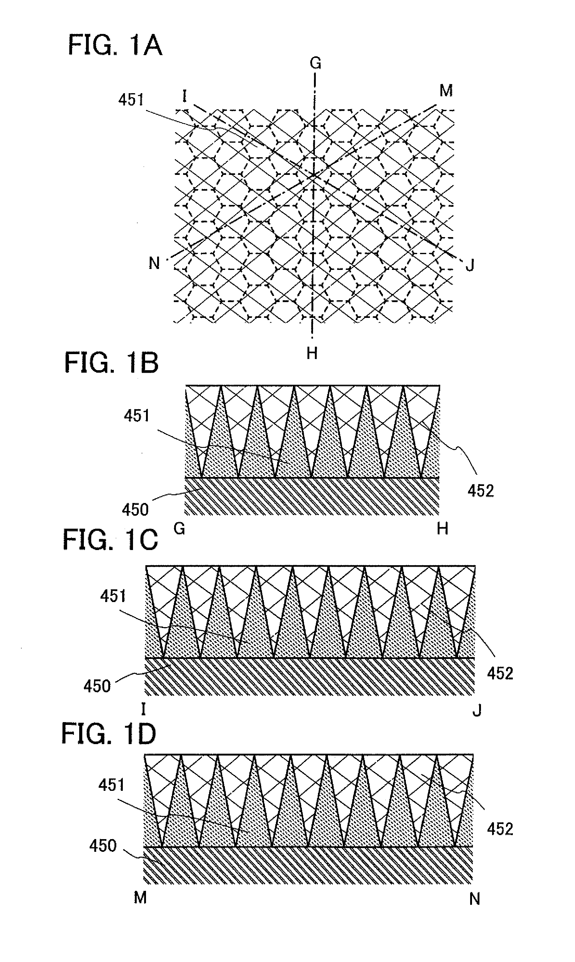
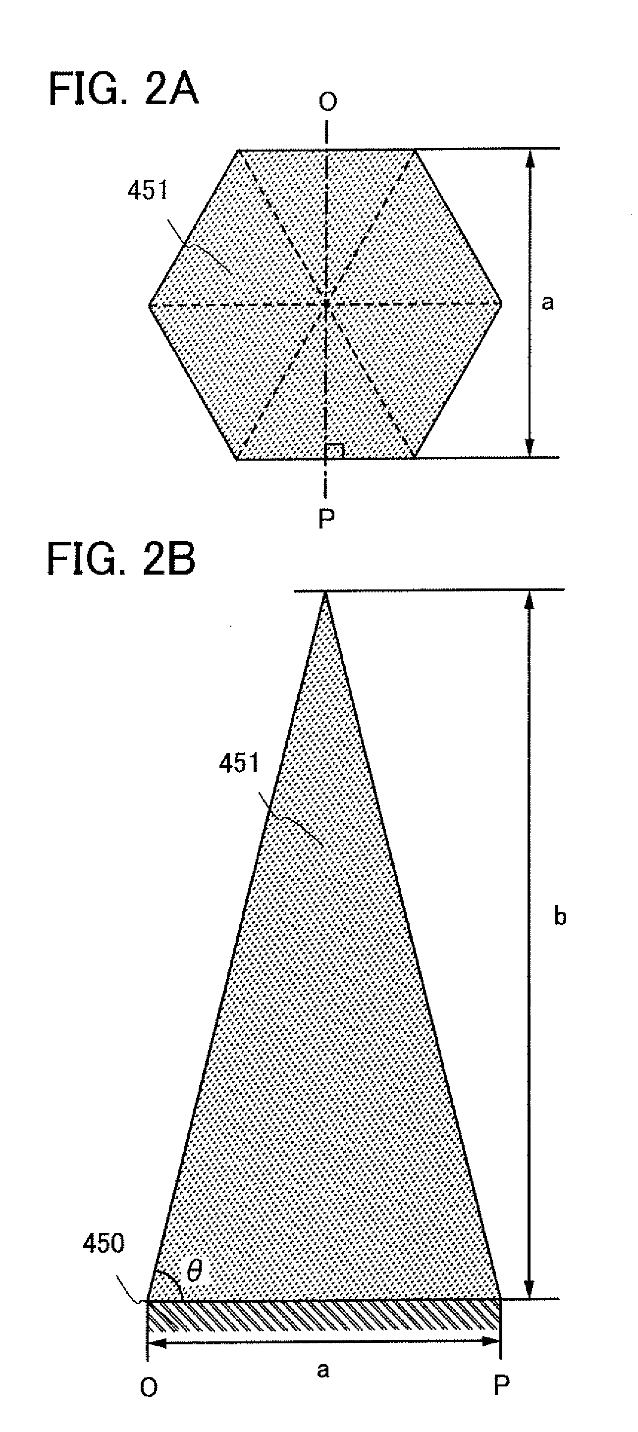
[0053]In this embodiment mode, an example of an anti-reflection layer for the purpose of having an anti-reflection function that can further reduce reflection of incident light from external and increasing visibility will be described.

[0054]FIG. 1A shows a top view of an anti-reflection layer of this embodiment mode that uses the present invention, and FIGS. 1B to 1D each show a cross-sectional view of an anti-reflection layer of this embodiment mode that uses the present invention. In FIGS. 1A to 1D, a plurality of hexagonal pyramidal projections 451 and a protective layer 452 are provided over a substrate that is to serve as a display screen of a PDP or an FED 450. The anti-reflection layer is formed of the plurality of hexagonal pyramidal projections 451 and the protective layer 452. FIG. 1A is a top view of a PDP or an FED of this embodiment mode. FIG. 1B is a cross-sectional view taken along line G-H from FIG. 1A. FIG. 1C is a cross-sectional view taken along line I-J from FIG....

embodiment mode 2

[0095]In this embodiment mode, an example of a PDP for the purpose of having an anti-reflection function that can further reduce reflection of incident light from external and increasing visibility will be described. That is, a structure of a PDP including a pair of substrates, a pair of electrodes provided between the pair of substrates, a phosphor layer provided between the pair of electrodes, and an anti-reflection layer provided on an outer side of one substrate of the pair of substrates will be described in detail.

[0096]In this embodiment mode, a surface emission PDP of an alternating current discharge type (an AC type) is shown. As shown in FIG. 9, in a PDP, a front substrate 110 and a back substrate 120 are placed facing each other, and the periphery of the front substrate 110 and the back substrate 120 is sealed with a sealant (not shown). In addition, a region enclosed by the front substrate 110, the back substrate 120, and the sealant is filled in with a discharge gas.

[009...

embodiment mode 3

[0148]In this embodiment mode, an FED for the purpose of having an anti-reflection function that can further reduce reflection of incident light from external and increasing visibility will be described. That is, a structure of an FED including a pair of substrates, a field emission element provided on one substrate of the pair of substrates, an electrode provided on the other substrate of the pair of substrates, a phosphor layer which comes into contact with the electrode, and an anti-reflection layer provided on an outer side of the other substrate will be described in detail.

[0149]The FED is a display device in which a phosphor is exited by an electron beam to emit light. The FED can be classified into a diode FED, a triode FED, and a tetrode FED according to the configuration of electrodes.

[0150]The diode FED has a structure where a rectangular cathode electrode is formed on a surface of a first substrate while a rectangular anode electrode is formed on a surface of a second sub...


PUM

PropertyMeasurementUnit
heightaaaaaaaaaa
heightaaaaaaaaaa
refractive indexaaaaaaaaaa

Abstract

It is an object to provide a plasma display and a field emission display that each have high visibility and an anti-reflection function that can further reduce reflection of incident light from external. Reflection of light can be prevented by having an anti-reflection layer that geometrically includes a plurality of adjacent pyramidal projections. In addition, a plurality of hexagonal pyramidal projections, each of which is provided with a protective layer formed of a material having a lower refractive index than a refractive index of the pyramidal projection so as to fill a space among the plurality of pyramidal projections, can be provided to be packed together without any spaces. Further, six sides of a pyramidal projection face different directions with respect to a base. Therefore, light can be diffused in many directions efficiently.

Description

TECHNICAL FIELD[0001]The present invention relates to a plasma display panel and a field emission display that each have an anti-reflection function.BACKGROUND ART[0002]In various displays (a plasma display panel (hereinafter referred to as a PDP), a field emission display (hereinafter referred to as an FED), and the like), there may be a case where it becomes difficult to see an image of a display screen due to reflection of its surroundings by surface reflection of incident light from external so that visibility is decreased. This is a considerable problem, particularly in regards to an increase in the size of the display device or outdoor use thereof.[0003]In order to prevent such reflection of incident light from external, a method for providing display screens of a PDP and an FED each having an anti-reflection film has been employed. For example, there is a method for providing an anti-reflective film that has a multilayer structure of stacked layers having different refractive...

Claims


Application Information

Patent Timeline
Patent Type & Authority Applications(United States)
IPC IPC(8): H01J1/62B32B7/02G02B1/11G02B1/118G02B1/14G09F9/00H01J11/44H01J29/89H01J31/12
CPCH01J11/12H01J11/44H01J29/86H01J2329/892H01J2211/442H01J2211/444H01J31/127
Inventor NISHIDA, JIROEGI, YUJINISHI, TAKESHIYAMAZAKI, SHUNPEI
Owner SEMICON ENERGY LAB CO LTD
Why Eureka
Try Eureka