

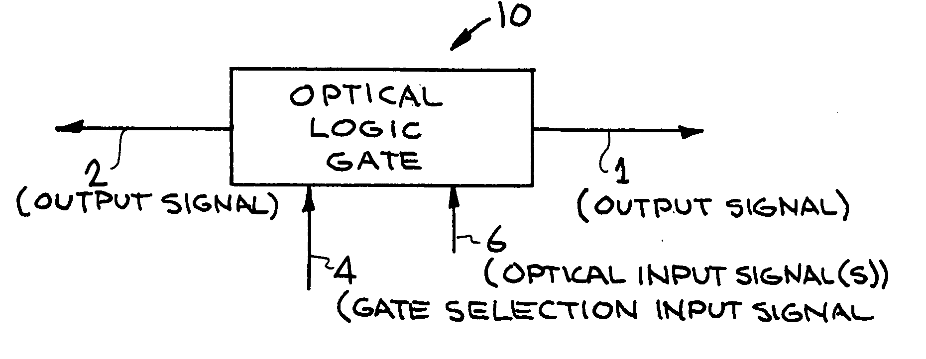
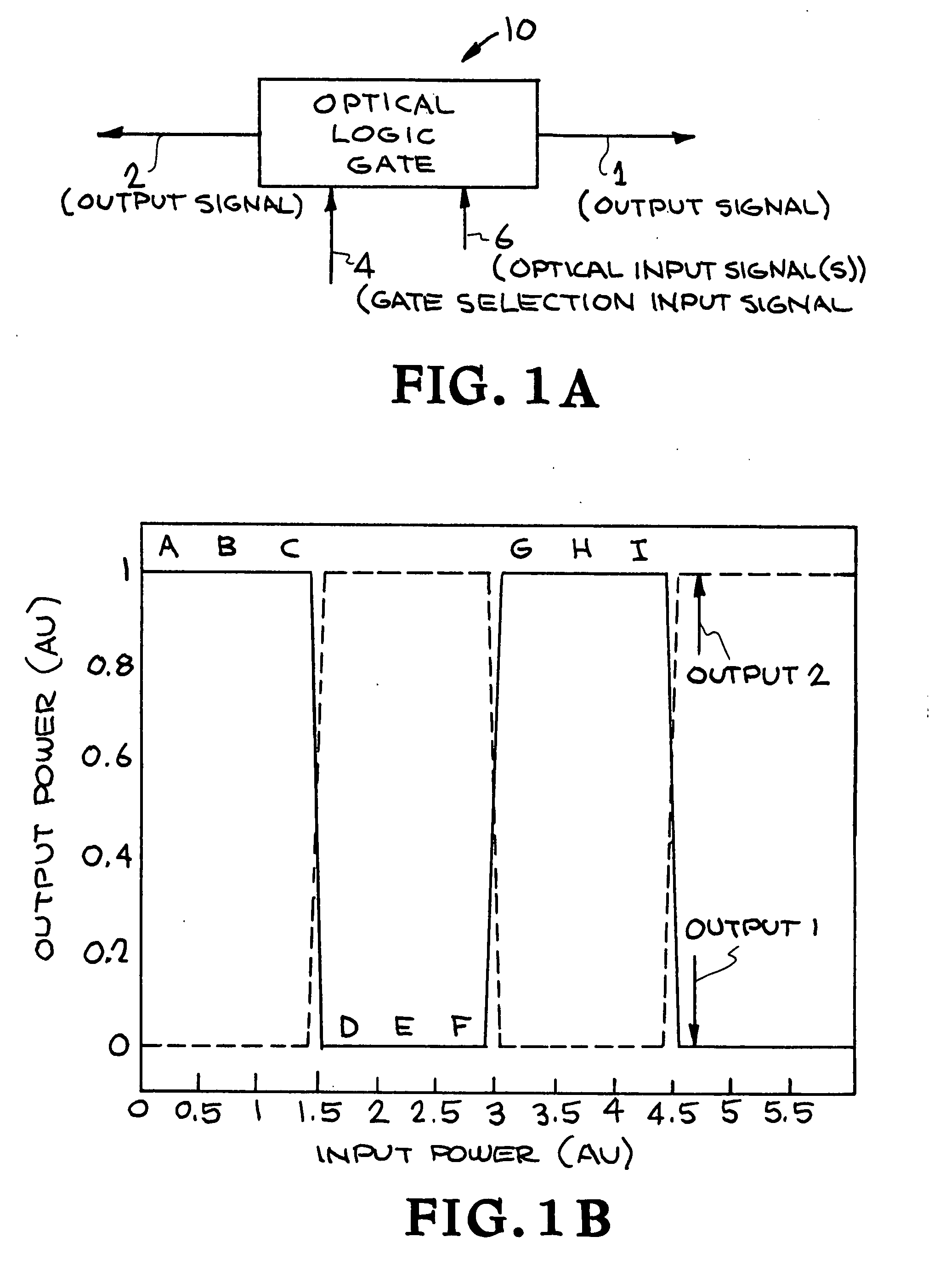
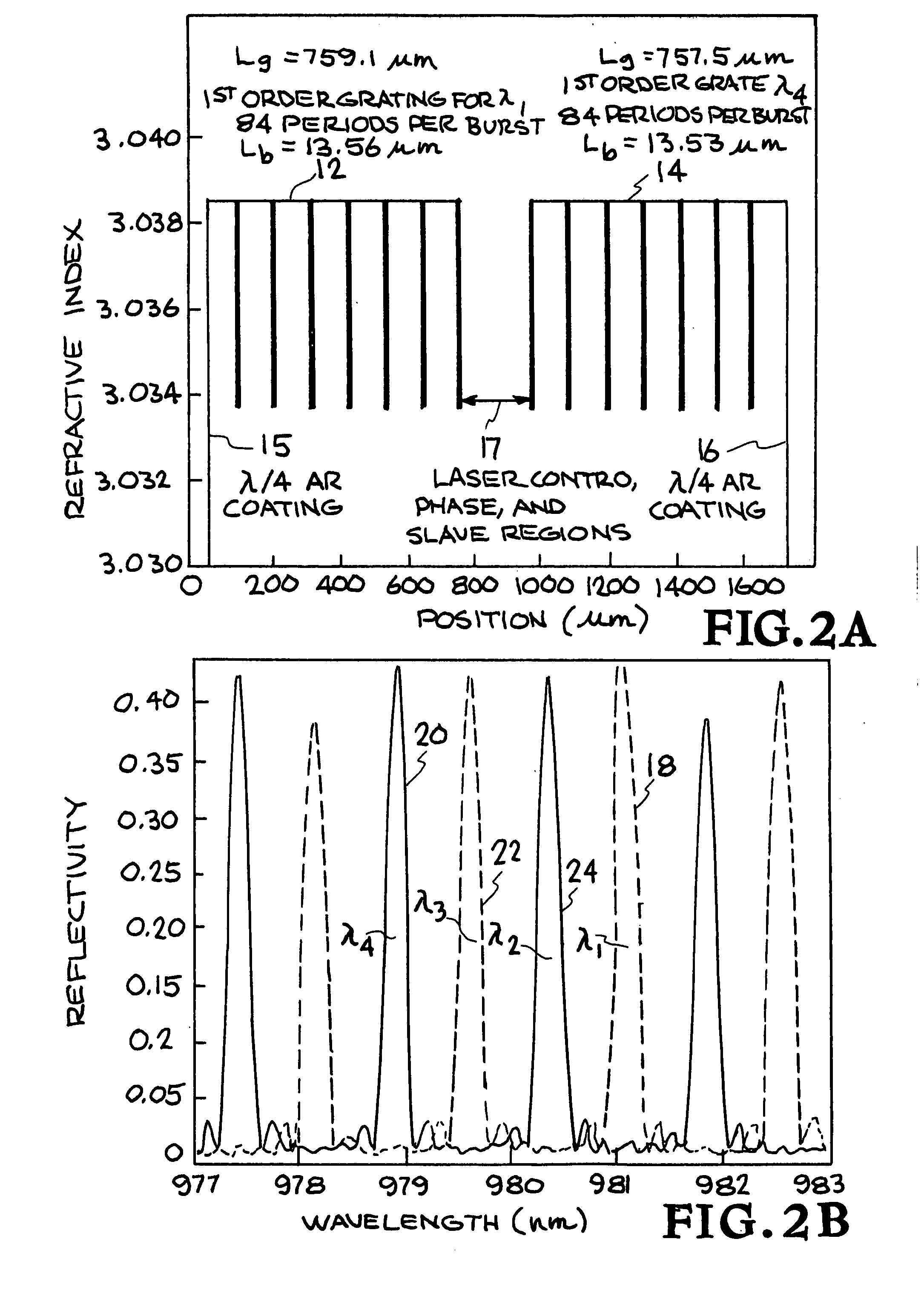
Rapidly reconfigurable all-optical universal logic gate
a universal logic gate, all-optical technology, applied in the direction of logic circuits, instruments, pulse techniques, etc., can solve the problems of limiting the operation speed of such devices, affecting the bit error rate, and taking an incredibly long time to turn back
- Summary
- Abstract
- Description
- Claims
- Application Information
AI Technical Summary
Benefits of technology
Problems solved by technology
Method used
Image

Examples
Embodiment Construction
[0021]Unless otherwise indicated, all numbers expressing quantities of ingredients, constituents, reaction conditions and so forth used in the specification and claims are to be understood as being modified in all instances by the term “about”. Accordingly, unless indicated to the contrary, the numerical parameters set forth in the specification and attached claims are approximations that may vary depending upon the desired properties sought to be obtained by the subject matter presented herein. At the very least, and not as an attempt to limit the application of the doctrine of equivalents to the scope of the claims, each numerical parameter should at least be construed in light of the number of reported significant digits and by applying ordinary rounding techniques. Notwithstanding that the numerical ranges and parameters setting forth the broad scope of the subject matter presented herein are approximations, the numerical values set forth in the specific examples are reported as...
PUM
| Property | Measurement | Unit |
|---|---|---|
| wavelengths | aaaaa | aaaaa |
| reflectivity | aaaaa | aaaaa |
| reflectivity | aaaaa | aaaaa |
Abstract
Description
Claims
Application Information