Method for forming hard mask patterns having a fine pitch and method for forming a semiconductor device using the same

a technology of hard mask patterns and semiconductor devices, which is applied in the direction of photomechanical devices, instruments, photosensitive material processing, etc., can solve the problems of potential pattern collapse, limited reduction of pitch between adjacent semiconductor patterns, and electrical failures

Active Publication Date: 2008-06-05
SAMSUNG ELECTRONICS CO LTD
View PDF18 Cites 63 Cited by
  • Summary
  • Abstract
  • Description
  • Claims
  • Application Information

AI Technical Summary

Benefits of technology

[0007]Embodiments of the present invention are therefore directed to a method for forming a hard mask with fine patterns and a method

Problems solved by technology

Reducing a pitch between adjacent semiconductor patterns may be limited when using a conventional photolithography process due to resolution restrictions, e.g., when forming a line and space (L/S) pattern on a substrate.
Further, con

Method used


Image

  • Method for forming hard mask patterns having a fine pitch and method for forming a semiconductor device using the same
  • Method for forming hard mask patterns having a fine pitch and method for forming a semiconductor device using the same
  • Method for forming hard mask patterns having a fine pitch and method for forming a semiconductor device using the same

Examples


Embodiment Construction

[0020]Korean Patent Application No. 10-2007-0068170, filed on Jul. 6, 2007, in the Korean Intellectual Property Office, and entitled, “Method for Forming Fine Pitch Hard Mask Pattern and Method for Fine Pattern of Semiconductor Device,” is incorporated by reference herein in its entirety.

[0021]Embodiments of the present invention will now be described more fully hereinafter with reference to the accompanying drawings, in which exemplary embodiments of the invention are illustrated. Aspects of the invention may, however, be embodied in different forms and should not be construed as limited to the embodiments set forth herein. Rather, these embodiments are provided so that this disclosure will be thorough and complete, and will fully convey the scope of the invention to those skilled in the art.

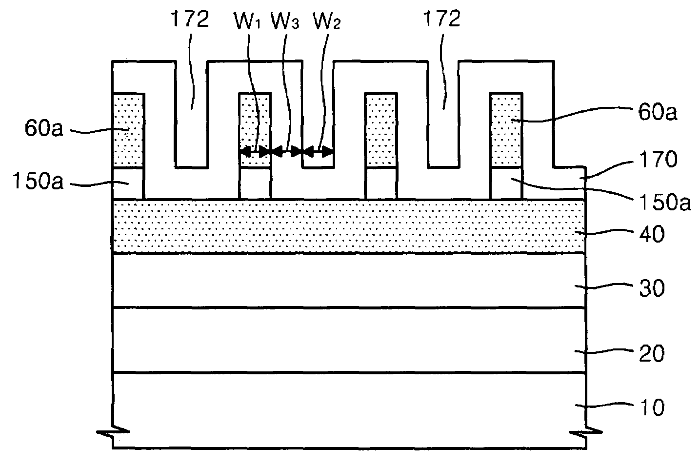
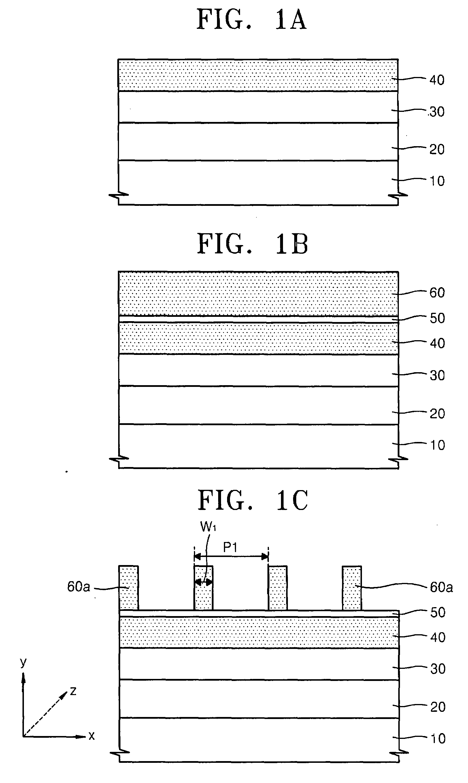
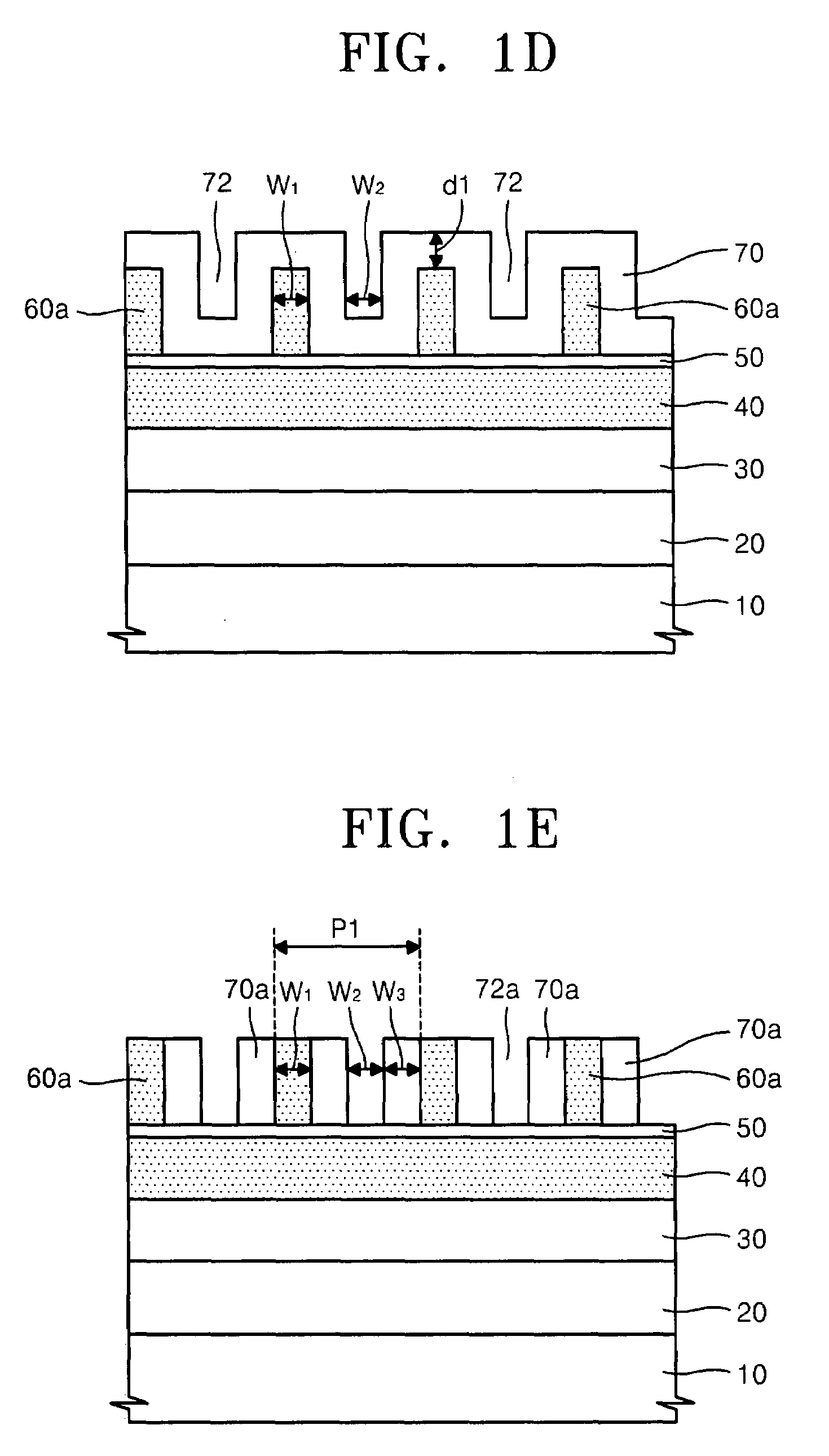
[0022]In the figures, the dimensions of layers and regions may be exaggerated for clarity of illustration. It will also be understood that when a layer or element is referred to as being “on” a...


PUM

PropertyMeasurementUnit
Thicknessaaaaaaaaaa
Heightaaaaaaaaaa

Abstract

A method for forming hard mask patterns includes, sequentially forming first, second, and third hard mask layers formed of materials having different etching selectivities on a substrate, forming first sacrificial patterns having a first pitch therebetween on the third hard mask layer, forming fourth hard mask patterns with a second pitch between the first sacrificial patterns, the second pitch being substantially equal to about ½ of the first pitch, patterning the third hard mask layer to form third hard mask patterns using the fourth hard mask patterns as an etch mask, patterning the second hard mask layer to form second hard mask patterns using the third and fourth hard mask patterns as an etch mask, and patterning the first hard mask layer to form first hard mask patterns with the second pitch therebetween using the second and third hard mask patterns as an etch mask.

Description

CROSS-REFERENCE TO RELATED APPLICATIONS[0001]The present application is a continuation-in-part application of co-pending U.S. patent application Ser. No. 11 / 367,437, entitled, “Method of Forming Pattern Using Fine Pitch Hard Mask,” which was filed on Mar. 6, 2006, co-pending U.S. patent application Ser. No. 11 / 896,512, entitled, “Method of Forming Fine Metal Patterns for a Semiconductor Device Using a Damascene Process,” which was filed on Sep. 4, 2007, and co-pending U.S. patent application Ser. No. ______, entitled, “Method for Forming Fine Patterns of a Semiconductor Device Using a Double Patterning Process,” which was filed on Oct. 30, 2007, which are all incorporated by reference herein in their entirety.BACKGROUND OF THE INVENTION[0002]1. Field of the Invention[0003]Embodiments of the present invention relate to a method for manufacturing a semiconductor device. More particularly, embodiments of the present invention relate to a method for forming hard mask patterns having a r...

Claims


Application Information

Patent Timeline
IPC IPC(8): G03F7/40G03F1/00
CPCH01L21/0337H01L21/3088H01L21/3086H01L21/0338
Inventor LEE, HAK-SUNKIM, MYEONG-CHEOLJEON, KYUNG-YUBKOH, CHA-WONLEE, JI-YOUNG
Owner SAMSUNG ELECTRONICS CO LTD
Why Eureka
Try Eureka