
Charged-Particle Beam System

a beam system and charge technology, applied in the direction of material analysis using wave/particle radiation, instruments, nuclear engineering, etc., can solve the problems of not being able to directly identify the physical position of a defective portion, unable to obtain the detection output, and becoming difficult to identify the defective portion with the above-described emission microscop

Inactive Publication Date: 2008-06-12
JEOL LTD
View PDF5 Cites 11 Cited by
  • Summary
  • Abstract
  • Description
  • Claims
  • Application Information

AI Technical Summary

Benefits of technology

[0011]It is an object of the present invention to provide a charged-particle beam system capable of detecting interconnect defects reliably.
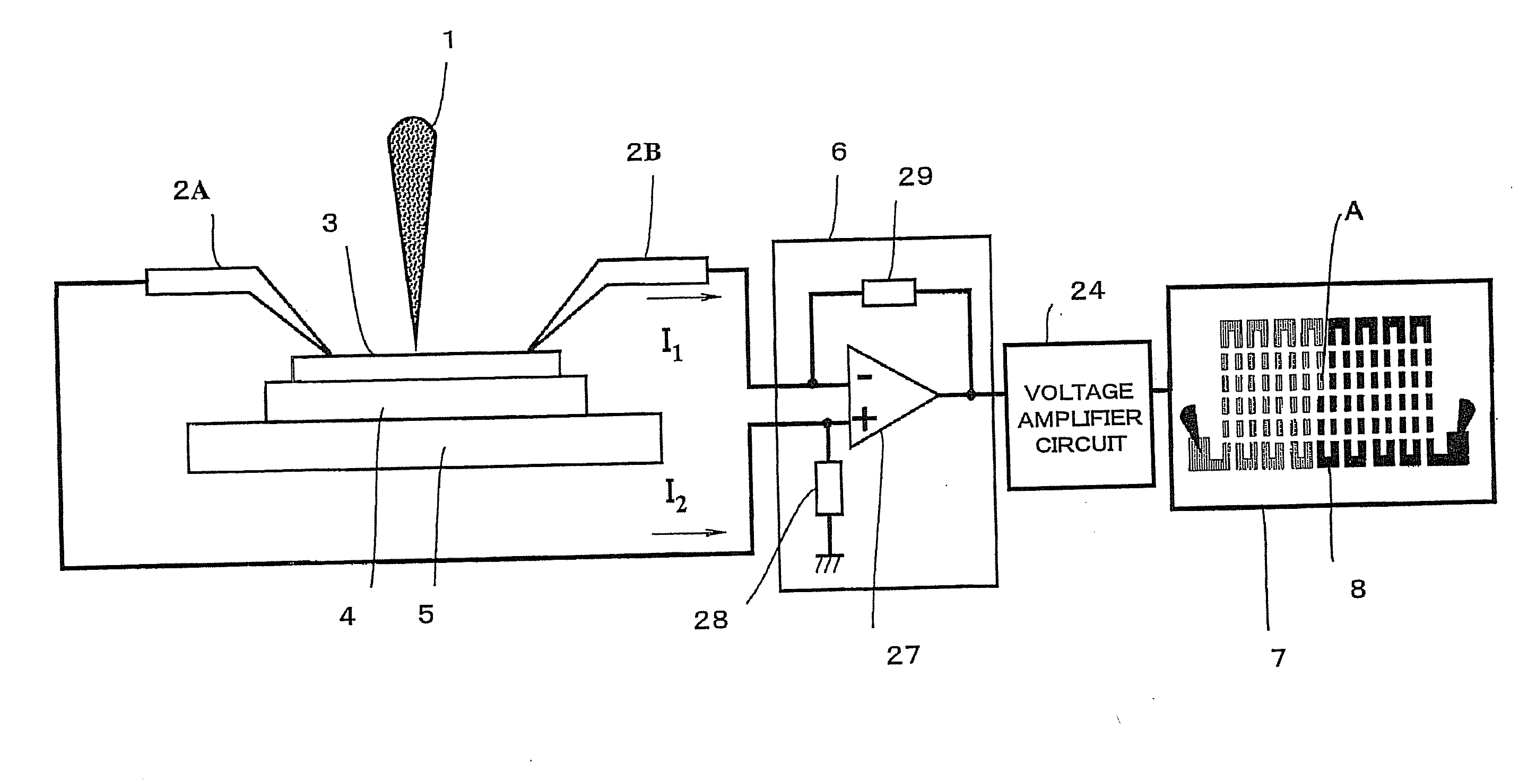
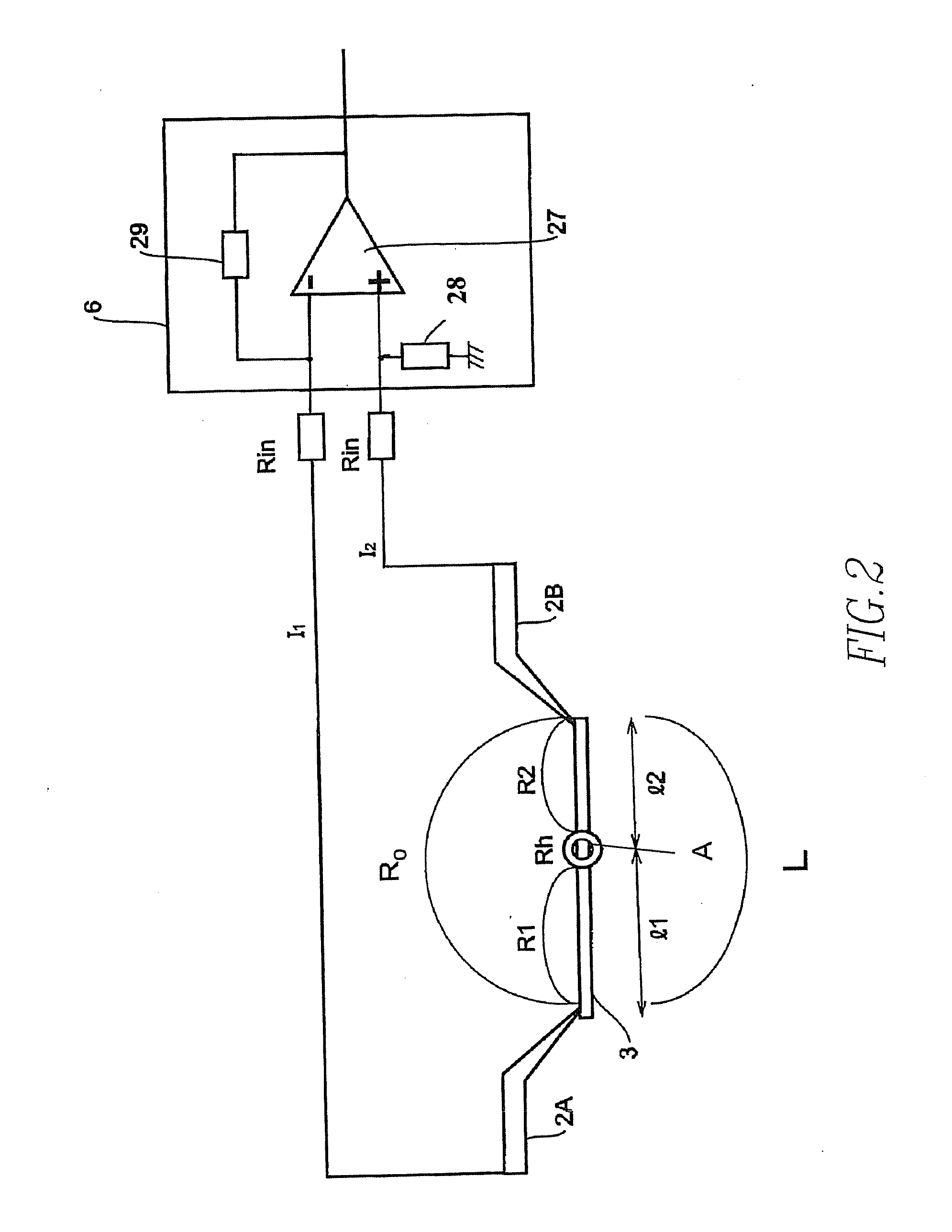
[0013]In the present invention, the absorption currents flowing through the first and second probes, respectively, are fed to the differential current-voltage converter. As a result, the difference between the absorption currents flowing through the first and second probes, respectively, is converted into a voltage signal. An absorption current image is created based on the voltage signal and displayed. Consequently, the contrast can be greatly accentuated across a defective portion in the interconnect pattern. As a result, the defective portion in the pattern can be detected reliably.

Problems solved by technology

However, in some cases, the physical position of a defective portion may not be directly identified because of insufficient resolution.
Furthermore, in recent years, conductive interconnects in semiconductor devices have been made finer and so it has become difficult to identify defective portions with the above-described emission microscopes.
As a result, no detection output is obtained.
Hence, there is the problem that it is impossible to identify the defective portion in the interconnect pattern.

Method used


Image

  • Charged-Particle Beam System
  • Charged-Particle Beam System
  • Charged-Particle Beam System

Examples


first embodiment

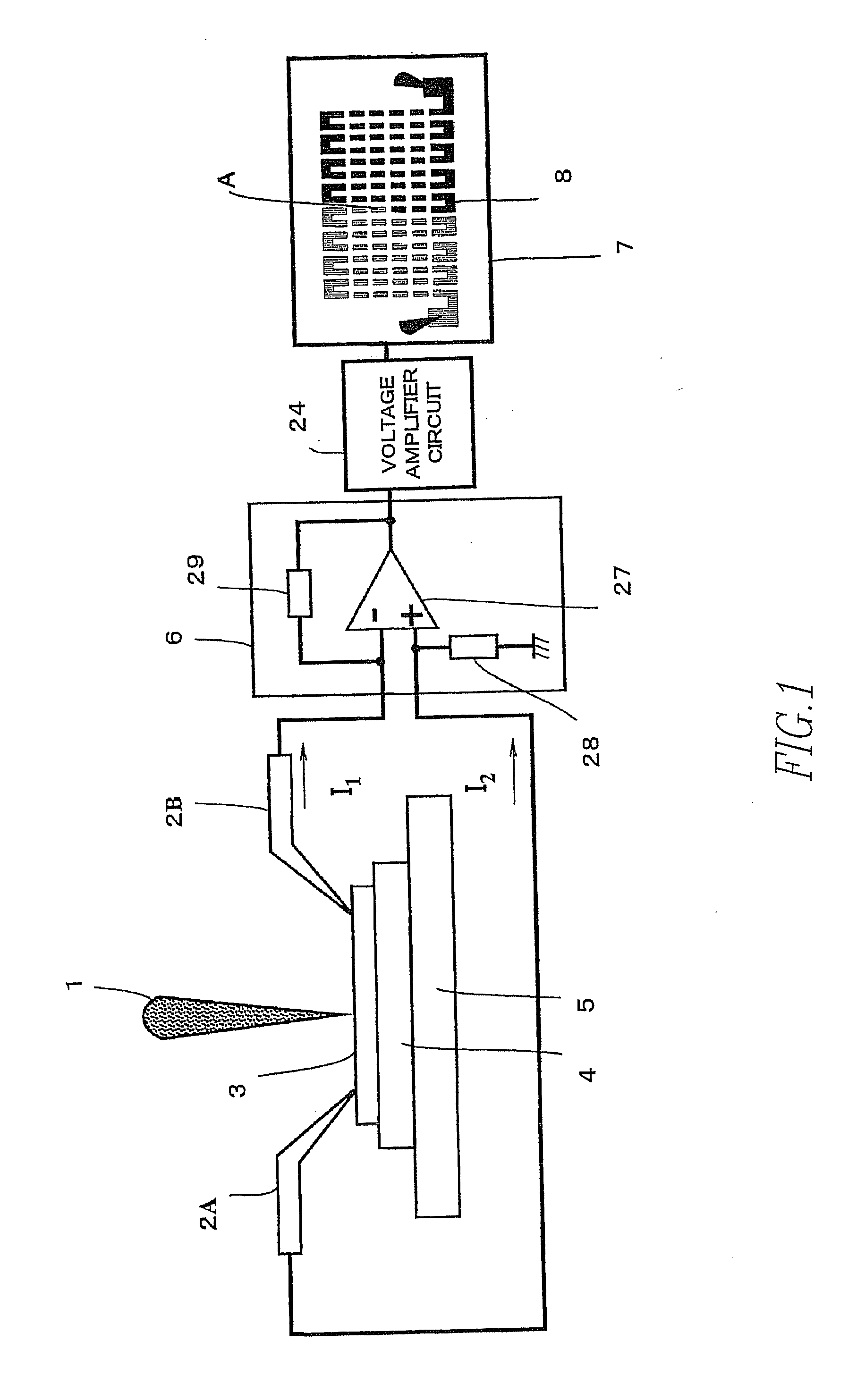
[0023]FIG. 1 is a schematic representation of a charged-particle beam system according to one embodiment of the present invention. Those components of FIG. 1 which are identical with their counterparts of FIG. 7 are indicated by the same reference numerals as in FIG. 7.

[0024]In FIG. 1, probes 2A and 2B are in contact with the opposite ends of an interconnect pattern 3 at their respective one ends, the pattern 3 being formed on a specimen 4. The other ends of the probes 2A and 2B are connected with a differential current-voltage converter 6. The converter 6 is made up of the operational amplifier 27, feedback resistor 29, and another resistor 28. The other end of the probe 2A is connected with the positive input terminal of the operational amplifier 27. The other end of the probe 2B is connected with the negative input terminal of the operational amplifier 27. The resistor 28 is connected between the positive input terminal of the amplifier 27 and ground.

[0025]In the operation of the...

second embodiment

[0050]FIG. 6 is a diagram showing main portions of a charged-particle beam system according to another embodiment of the present invention. Those components of FIG. 6 which are identical with their counterparts of FIG. 1 are indicated by the same reference numerals as in FIG. 1.

[0051]A Fourier transform circuit 20 Fourier transforms the output signal from the differential current-voltage converter 6. A frequency identification means 21 identifies the frequencies of the output signal from the Fourier transform circuit 20. An inverse Fourier transform circuit 22 inverse Fourier transforms the output signal from the frequency identification means 21.

[0052]The operation of the system constructed in this way is described. The probes 2A and 2B are brought into contact with the opposite ends of the interconnect pattern 3 formed on the specimen 4 which, in turn, is placed on the specimen stage 5. Under this condition, the electron beam 1 is scanned over the surface of the specimen 4. An abs...


PUM

PropertyMeasurementUnit
absorption currentaaaaaaaaaa
absorption current imageaaaaaaaaaa
absorption currentaaaaaaaaaa

Abstract

A charged-particle beam system capable of reliably detecting defects in an interconnect pattern, which is formed, for example, on a semiconductor device. The system uses an electron source for producing an electron beam. A specimen on which the interconnect pattern is formed is scanned with the electron beam in two dimensions. An image of the specimen is created based on a signal obtained from the specimen in response to the scanning, and the image is displayed on a display portion. Two probes are brought into contact with arbitrary locations on the interconnect pattern. Absorption currents obtained via the probes are applied to a differential current-voltage converter. Thus, the difference between the absorption currents is converted into a voltage signal. An absorption current image is created based on the voltage signal and displayed on the display portion.

Description

BACKGROUND OF THE INVENTION[0001]1. Field of the Invention[0002]The present invention relates to a charged-particle beam system capable of identifying defective portions of a specimen.[0003]2. Description of Related Art[0004]Emission microscopes are used in failure analysis of semiconductor devices. However, in some cases, the physical position of a defective portion may not be directly identified because of insufficient resolution. Furthermore, in recent years, conductive interconnects in semiconductor devices have been made finer and so it has become difficult to identify defective portions with the above-described emission microscopes.[0005]In recent years, a charged-particle beam system for performing failure analysis of a semiconductor device by irradiating the surface of the device with a charged-particle beam, detecting the electrical current absorbed into the interconnect pattern, and imaging the detected current has attracted attention.[0006]FIG. 7 shows one example of the ...

Claims


Application Information

Patent Timeline
Patent Type & Authority Applications(United States)
IPC IPC(8): G21K5/04G01N23/08
CPCG01N23/2251H01J37/244H01J2237/24592H01J2237/24564H01J37/252
Inventor ETO, YOSHIYUKI
Owner JEOL LTD
Learn More