Semiconductor device and method for fabricating the same

a technology of semiconductor devices and semiconductors, applied in semiconductor devices, electrical equipment, transistors, etc., can solve the problems of easy failure of the metal film deposited in the opening portion, difficult formation of a uniform silicide layer on the gate electrode b>4/b>, and defective transistor characteristics, etc., to achieve the effect of reducing resistance and widening the opening portion in the gate length direction

Inactive Publication Date: 2008-06-12
PANASONIC CORP
View PDF7 Cites 7 Cited by
  • Summary
  • Abstract
  • Description
  • Claims
  • Application Information

AI Technical Summary

Benefits of technology

[0029]According to the method, by removing part of the second sidewall film as well as the first insulation film, a width of the opening portion in the gate length direction can be increased by an amount corresponding to a width of the second sidewall film. Thus, compared to the first method for fabricating a semiconductor device according to the present invention, the metal film can be deposited more uniformly. Therefore, a gate electrode which is formed of uniform metal silicide and of which resistance is reduced can be formed.

Problems solved by technology

In the step (FIG. 5F) of depositing a metal film in the opening portion which reaches the gate electrode 4, if the opening portion has an increased aspect ratio with reduction in the size of semiconductor devices, a coverage failure of the metal film deposited in the opening portion easily occurs and formation of a uniform silicide layer on the gate electrode 4 becomes difficult.
As a result, defective transistor characteristics, quality variations and the like might be increased.

Method used


Image

  • Semiconductor device and method for fabricating the same
  • Semiconductor device and method for fabricating the same
  • Semiconductor device and method for fabricating the same

Examples


first embodiment

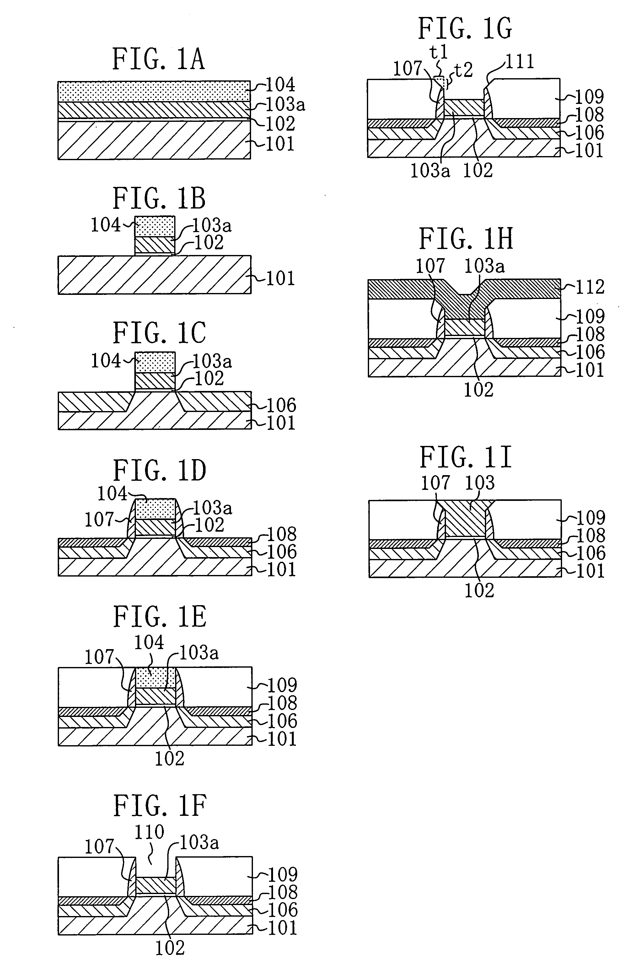
[0035]Hereafter, a semiconductor device according to a first embodiment of the present invention and a method for fabricating the semiconductor device will be described with reference to the accompanying drawings. FIGS. 1A through 1I are cross-sectional views illustrating respective steps for fabricating a semiconductor device according to the first embodiment of the present invention. First, a structure of the semiconductor device of this embodiment will be briefly described with reference to FIG. 1I.

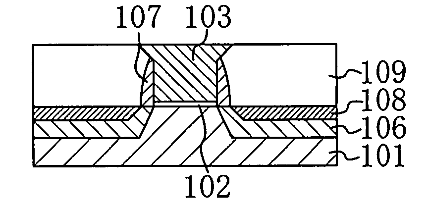
[0036]As shown in FIG. 1I, the semiconductor device of this embodiment includes a semiconductor substrate 101 of silicon or the like, low concentration source / drain regions 106 and high concentration source / drain regions 108 each being formed in the semiconductor substrate 101, a gate insulation film 102 formed in part of the semiconductor substrate 101 located between the low concentration source / drain regions is 106 when viewed from the top, a gate electrode 103 formed of metal silic...

second embodiment

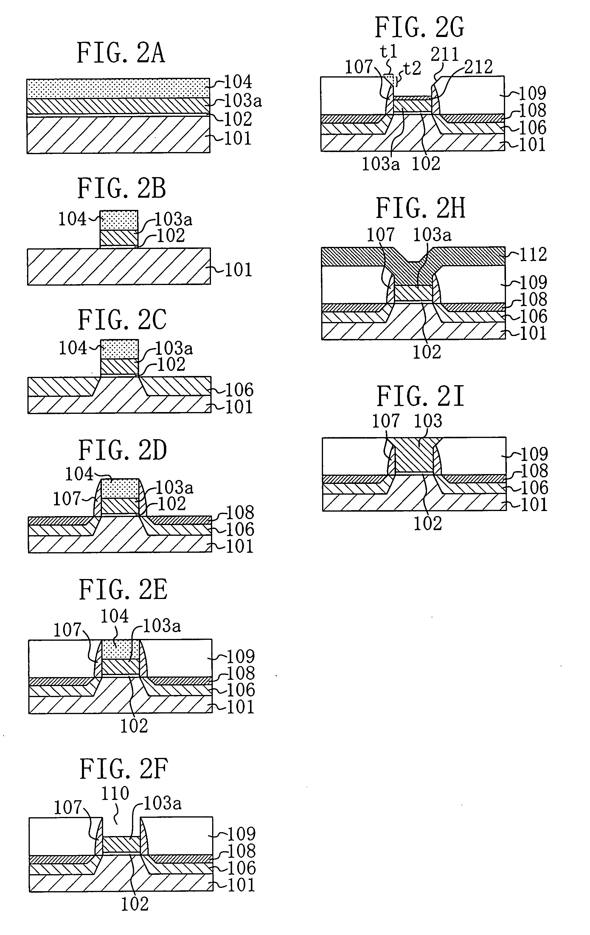
[0055]Hereafter, a method for fabricating a semiconductor device according to a second embodiment of the present invention will be described with reference to the accompanying drawings. A semiconductor device according to this embodiment has a similar structure to the structure of the semiconductor device of the first embodiment but part of the method for fabricating a semiconductor device according to this embodiment is different from the method for fabricating a semiconductor device according to the first embodiment. Therefore, in this embodiment, the structure of the semiconductor device will be omitted. FIGS. 2A through 2I are cross-sectional views illustrating respective steps for fabricating a semiconductor device according to the second embodiment of the present invention. Except for the step of FIG. 2G, process steps of the fabrication method of the second embodiment are the same as those of the fabrication method of the first embodiment and therefore will be briefly describ...

third embodiment

[0065]Hereafter, a semiconductor device according to a third embodiment of the present invention and a method for fabricating the semiconductor device will be described with reference to the accompanying drawings. FIGS. 3A through 3I are cross-sectional views illustrating respective steps for fabricating a semiconductor device according to the third embodiment of the present invention. First, a structure of the semiconductor device of this embodiment will be described with reference to FIG. 3I.

[0066]As shown in FIG. 3I, the semiconductor device of this embodiment includes a semiconductor substrate 101 of silicon or the like, low concentration source / drain regions 106 and high concentration source / drain regions 108 each being formed in the semiconductor substrate 101, a gate insulation film 102 formed in part of the semiconductor substrate 101 located between the low concentration source / drain regions 106 when viewed from the top, a gate electrode 303 formed of metal silicide on the ...


PUM


Abstract

A semiconductor device includes low concentration source/drain regions and high concentration source/drain regions each being formed in a semiconductor substrate, a gate insulation film formed on part of the semiconductor substrate located between the low concentration source/drain regions when viewed from the top and a gate electrode formed of metal silicide on the gate insulation film. A gate length of upper part of the gate electrode is larger than a gate length of other part of the gate electrode.

Description

BACKGROUND OF THE INVENTION[0001]1. Field of the Invention[0002]The present invention relates to a semiconductor device including a gate electrode with a silicide layer and a method for fabricating the semiconductor device.[0003]2. Description of the Prior Art[0004]In recent years, as effective means for realizing increased speed of semiconductor integrated circuit devices, a method in which high-melting point metal silicide is formed on a gate electrode to reduce resistances of the electrode and a doped layer has been used. Hereafter, the known method in which a silicide layer is formed on a gate electrode will be described with reference to FIG. 5. FIG. 5 is a cross sectional view illustrating a known method for forming a silicide layer.[0005]First, as shown in FIG. 5A, a field oxide film 2 is formed in an inert region of a silicon substrate 1 and a gate oxide film 3 having a thickness of 5-10 nm is formed in an active region of the silicon substrate 1 using respective known techn...

Claims


Application Information

Patent Timeline
Patent Type & Authority Applications(United States)
IPC IPC(8): H01L29/94H01L21/336
CPCH01L21/28097H01L21/28114H01L29/42376H01L29/7833H01L29/66545H01L29/66583H01L29/6659H01L29/4975
Inventor KOROGI, HAYATO
Owner PANASONIC CORP
Why Eureka
Try Eureka