Optical semiconductor device and optical waveguide

a technology of optical waveguide and optical semiconductor, which is applied in the direction of semiconductor lasers, instruments, optical elements, etc., can solve the problem of optical loss induced

Inactive Publication Date: 2008-06-12
HITACHI LTD
View PDF9 Cites 37 Cited by
  • Summary
  • Abstract
  • Description
  • Claims
  • Application Information

AI Technical Summary

Benefits of technology

[0019]According to the present invention, optical coupling of an optical waveguide with an optical waveguide

Problems solved by technology

However, the above-described structure has a problem that an optical loss is ind

Method used


Image

  • Optical semiconductor device and optical waveguide
  • Optical semiconductor device and optical waveguide
  • Optical semiconductor device and optical waveguide

Examples


embodiment 1

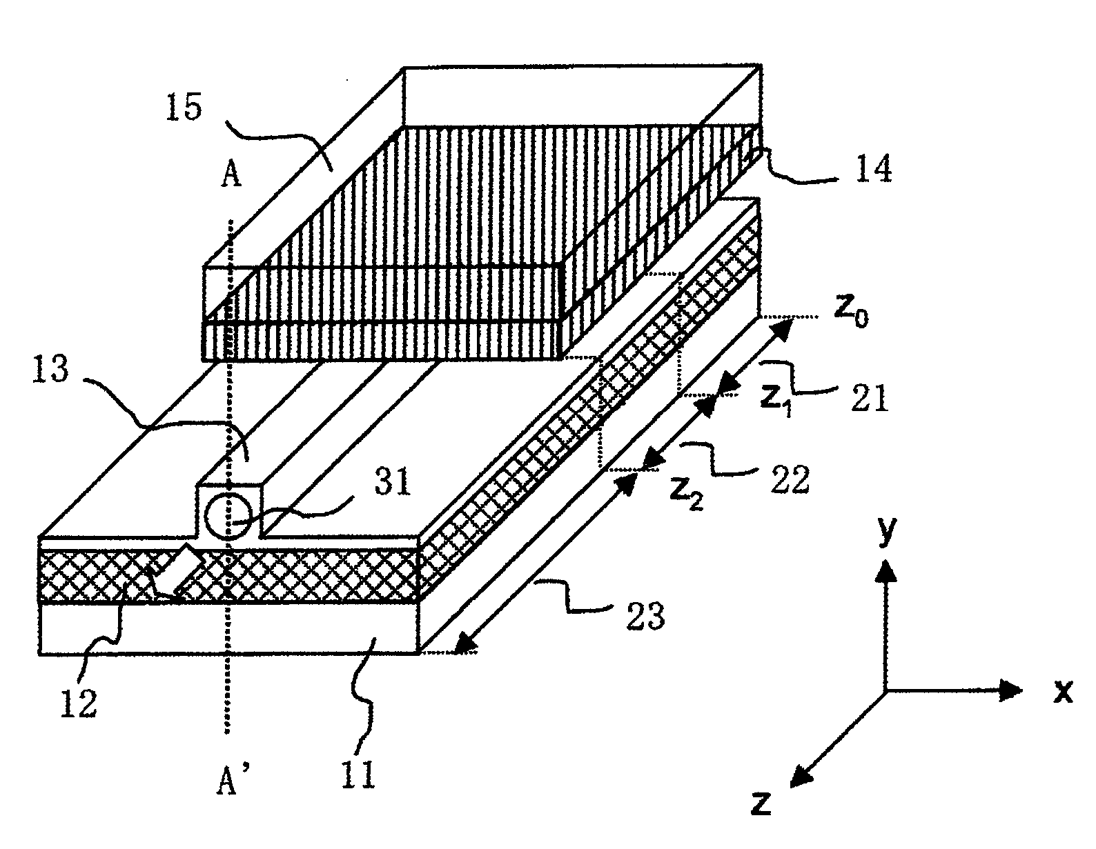
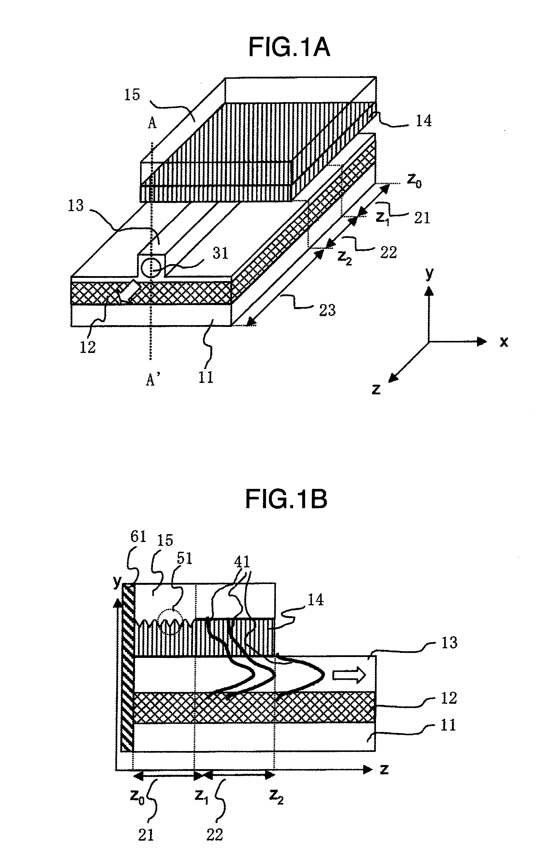
[0047]FIGS. 1A, 1B show a first embodiment of the invention. FIG. 1A shows a perspective view, and FIG. 1B shows a y-z cross-sectional view taken along A-A′ of FIG. 1A. This device comprises a resonator region 21 of a semiconductor laser, a mode conversion region 22 and a Si wire region 23. The resonator region 21 has a Si substrate 11, a Si oxide film layer 12, a Si core layer 13, a compound semiconductor core layer 14 and a compound semiconductor substrate 15 stacked in this order from bottom to top. Here, refractive index n1 of the Si oxide film layer 12 is lower than refractive index n2 of the compound semiconductor core layer 14, and the refractive index n2 of the compound semiconductor core layer 14 is lower than refractive index n3 of the Si core layer 13, indicating n123. Further, in the resonator region 21, a grating 51 is formed between the compound semiconductor core layer 14 and the compound semiconductor substrate 15, and a high reflection coating 61 is formed on an end...

embodiment 2

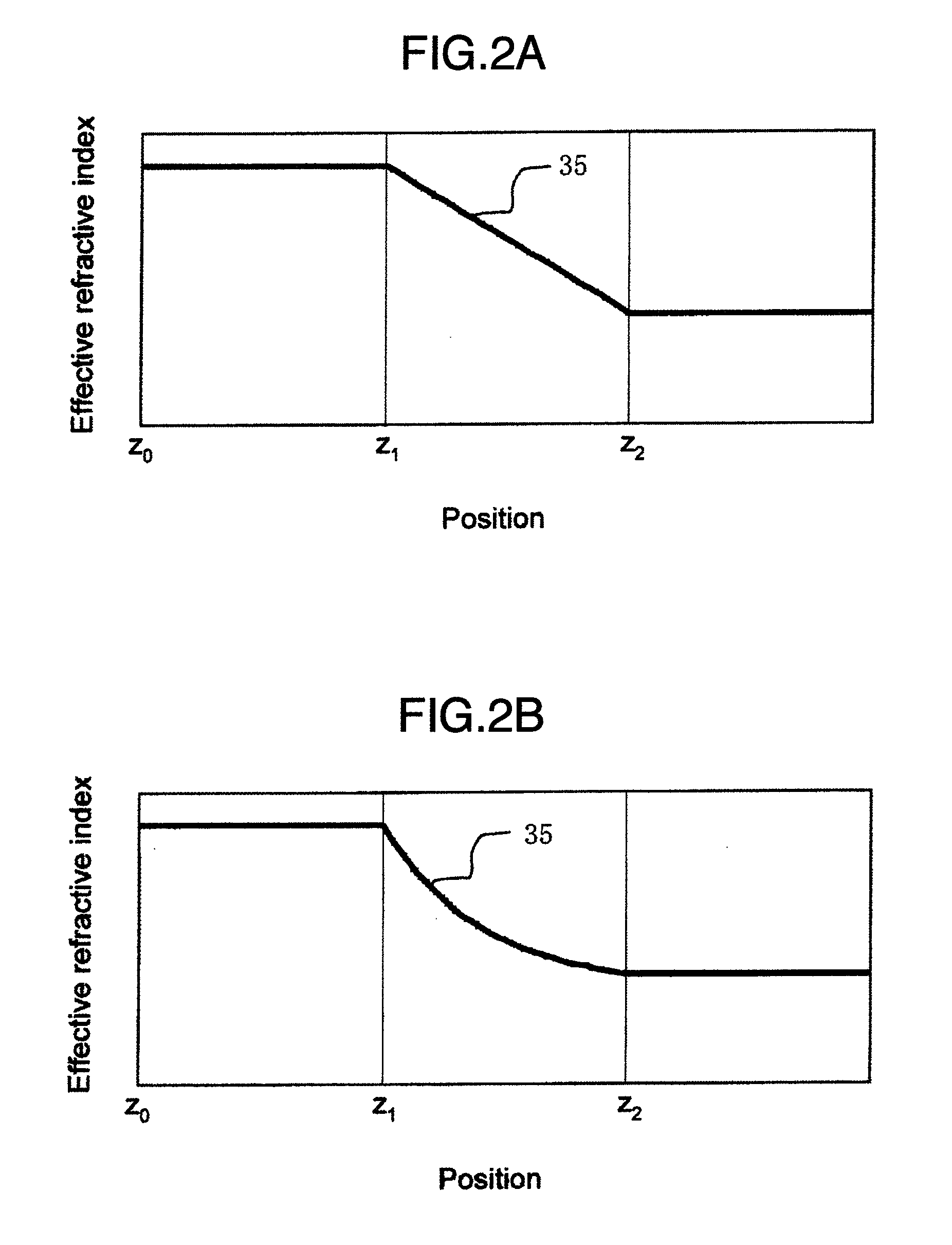
[0054]FIG. 5 shows a second embodiment of the invention. In this embodiment, a refractive index is adjusted by fabricating the compound semiconductor core layer 14 to have tapered shapes on the mode conversion region 22.

[0055]First, a method of producing the effective refractive index distribution shown in FIG. 2A or FIG. 2B by fabricating the compound semiconductor core layer 14 to have a tapered shape is described. The effective refractive index of the compound semiconductor core layer 14 becomes smaller as the stripe width becomes smaller. Therefore, as shown in FIG. 6A or FIG. 6B, the effective refractive index distribution shown in FIG. 2A or FIG. 2B can be produced on the compound semiconductor core layer 14 by adjusting a stripe width 38 of the compound semiconductor core layer 14 to have a tapered shape along the stripe direction of the Si core layer 13. FIG. 7 shows a production method of this embodiment. First, a compound semiconductor portion and a Si waveguide portion ar...

embodiment 3

[0058]FIG. 10 shows a third embodiment of the invention. In this embodiment, the refractive index is varied by making the end surface of the compound semiconductor core layer 14 crossed with side walls 13-1 of the optical waveguide stripe in the mode conversion region 22. The device explained in this embodiment can be easily fabricated because it does not require fine-pattern fabrication techniques to fabricate the compound semiconductor core layer 14.


PUM


Abstract

A core of an optical waveguide and a core of a waveguide type optical device are adjacently disposed, and a layer is continuously formed at one end of the core of the waveguide type optical device, wherein an effective refractive index of the layer decreases toward a long axis direction of the optical waveguide stripe.

Description

INCORPORATION BY REFERENCE[0001]The present application claims priority from Japanese application JP-A-2006-328938 filed on Dec. 6, 2006, the content of which is hereby incorporated by reference into this application.BACKGROUND OF THE INVENTION[0002]The present invention relates to an optical semiconductor device and an optical waveguide, and more particularly to a technology of coupling optical waveguides mutually without a large optical loss.[0003]Demands for a large capacity optical communication device are increasing with a recent increase in communication traffic. Therefore, miniaturization of optical components effective in increasing the capacity of the device is being studied vigorously at various places. For example, a technology of using a Si wire in order to miniaturize an optical waveguide circuit is being studied. The Si wire optical waveguide confines light within the core more strongly in comparison with a conventional case that Silica glass or polymer is used. Theref...

Claims


Application Information

Patent Timeline
IPC IPC(8): H01S5/026G02B6/10H01S5/12
CPCG02B6/1228G02B6/125H01S5/021H01S5/3224H01S5/028H01S5/1014H01S5/12H01S5/026H01S3/094G02B6/12
Inventor TAKAHASHI, MAKOTOARIMOTO, HIDEOHOSOMI, KAZUHIKOFUKAMACHI, TOSHIHIKOMAKINO, SHIGEKIMATSUOKA, YASUNOBUSUGAWARA, TOSHIKI
Owner HITACHI LTD
Why Eureka
Try Eureka