Solid-state image pickup apparatus and electronic apparatus

a pickup apparatus and solid-state technology, applied in the direction of solid-state devices, color television, television systems, etc., can solve the problems of loss of a light amount corresponding, loss of a degree of freedom of the layout of a photoelectric converter or a pixel transistor on a substrate, and deviation of an incident light part, so as to reduce the total the loss of the light amount in the path between the lens and the photoelectric converter

Active Publication Date: 2010-08-05
SONY SEMICON SOLUTIONS CORP
View PDF5 Cites 10 Cited by
  • Summary
  • Abstract
  • Description
  • Claims
  • Application Information

AI Technical Summary

Benefits of technology

[0010]For example, when the center of the entire waveguide is shifted from the main light beam that passes the center of the lens in the direction in which the area where the waveguide is overlapped with the photoelectric converter is increased, the loss of the light amount generated between the lens and the waveguide is slightly larger than the case where the center of the entire waveguide is coincided with the center of the lens. But, because the area where the waveguide is overlapped with the photoelectric converter is large, light confined in the waveguide is efficiently guided to the light reception surface of the photoelectric converter.
[0011]In this case, the loss of the light amount generated between the waveguide and the photoelectric converter is smaller than the loss of the light amount between the waveguide and the photoelectric converter in a case where the gravity center of the area of the photoelectric converter is shifted from the center of the lens or the waveguide. Therefore, by using the structure in which the center of the waveguide is shifted from the main light beam that passes the center of the lens in the direction in which the area where the waveguide is overlapped with the photoelectric converter is increased, the total loss of the light amount in the path (optical path) between the lens and the photoelectric converter can be reduced.
[0012]According to the present invention, the loss of the light amount in the path between the lens and the photoelectric converter can be reduced as compared to the case where the gravity center of the area of the photoelectric converter is shifted from the center of the lens or the waveguide.

Problems solved by technology

When a pixel size is increasingly miniaturized in a solid-state image pickup apparatus of the surface incident type, a degree of freedom of a layout of a photoelectric converter or a pixel transistor on a substrate is lost.
As a result, in a solid-state image pickup apparatus having a waveguide structure, a gravity center of an area of a photoelectric converter is shifted from a center of a waveguide or a micro lens, which causes a loss of a light amount corresponding to such an extent that a part of incident light deviates from the area of a photoelectric converter.

Method used


Image

  • Solid-state image pickup apparatus and electronic apparatus
  • Solid-state image pickup apparatus and electronic apparatus
  • Solid-state image pickup apparatus and electronic apparatus

Examples


first embodiment

2. First Embodiment

(Pixel Structure)

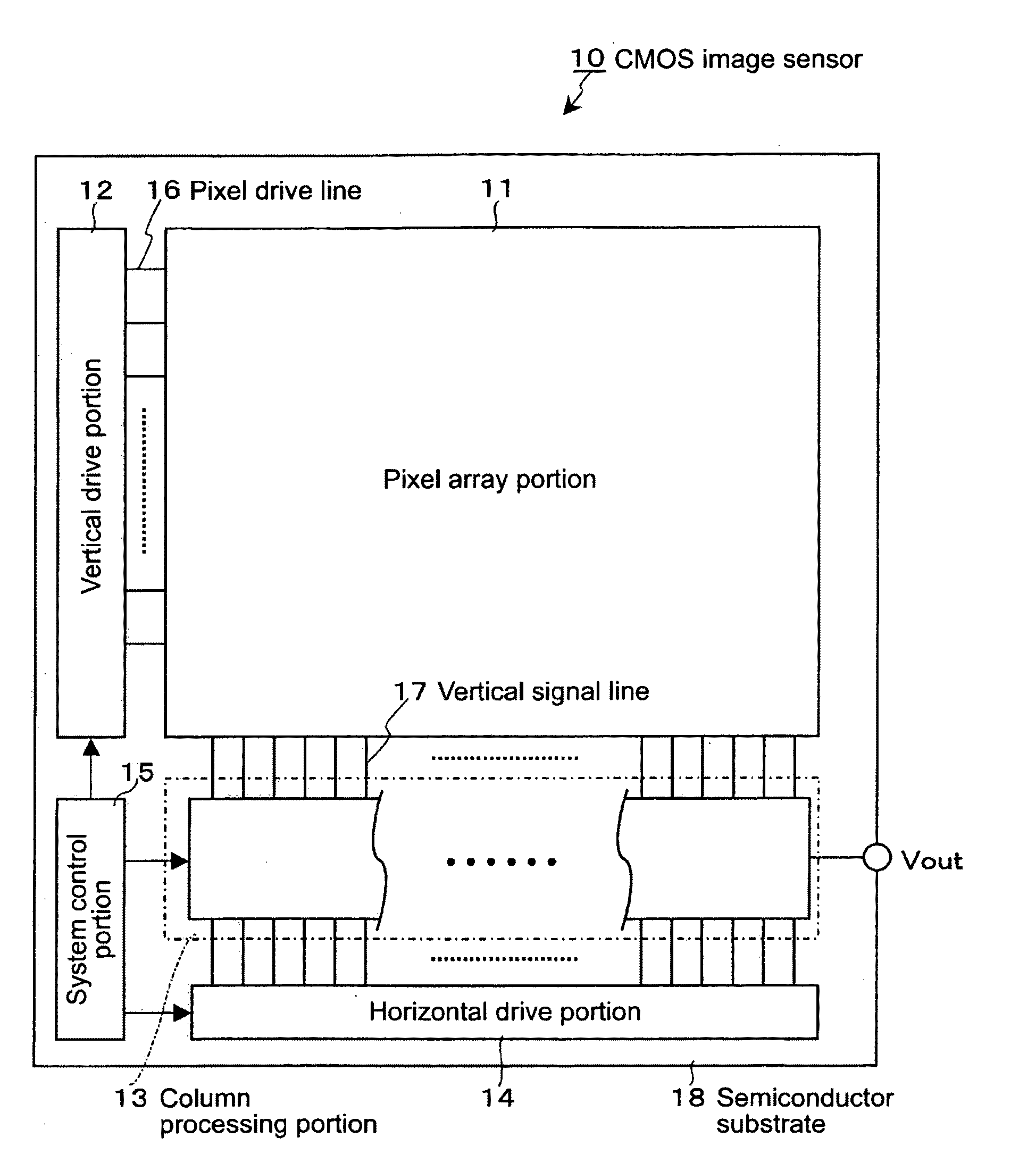
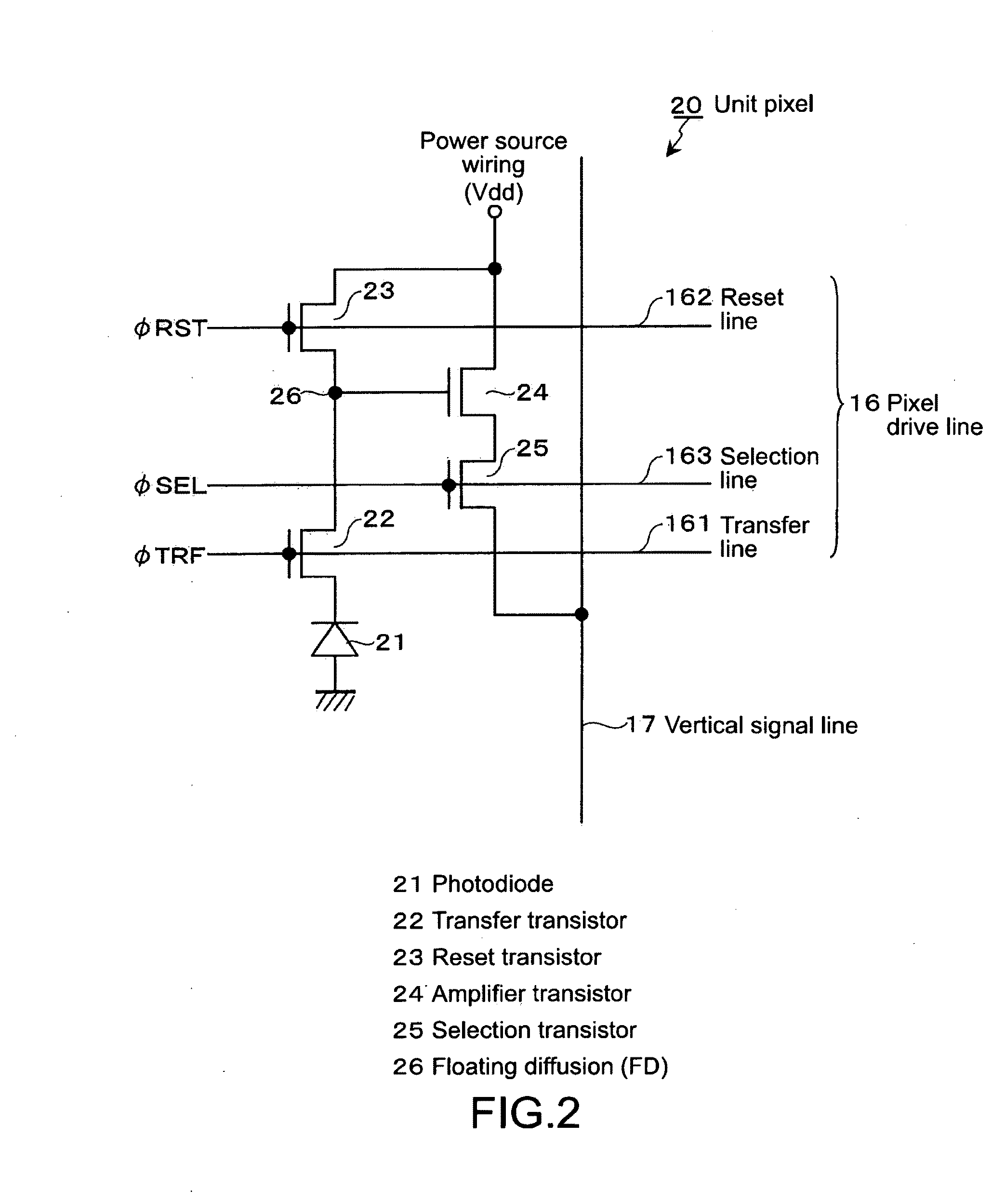
[0061]FIG. 3 is a cross-sectional view showing a cross-sectional structure of a pixel having a waveguide structure according to a first embodiment of the present invention. Here, for simplification of the figure, the waveguide structure of a certain unit pixel 20 that is disposed in the center portion of the pixel array portion 11 is shown. FIG. 4 is a diagram showing a positional relationship among a micro lens, a waveguide, and a photodiode in the waveguide structure according to the first embodiment.

[0062]In FIG. 3, in a subsurface portion of a semiconductor substrate, for example, a silicon substrate 31, a light reception sensor portion (photoelectric converter) 32 that performs photoelectric conversion is formed. The light reception sensor portion 32 is formed as a diode (that corresponds to the photodiode 21 shown in FIG. 2) constituted of a P-type diffusion layer and an N-type diffusion layer on a surface side thereof, for example. The ligh...

second embodiment

3. Second Embodiment

(Pixel Structure)

[0088]FIG. 10 is a cross-sectional view showing a cross-sectional structure of a pixel having a waveguide structure according to a second embodiment of the present invention. In FIG. 10, the same components shown in FIG. 3 are denoted by the same reference numerals or symbols.

[0089]Here, for simplification of the figure, the waveguide structure of the certain unit pixel 20 that is disposed in the center portion of the pixel array portion 11 is shown. FIG. 11 is a diagram showing a positional relationship among the micro lens, the waveguide, and the photodiode in the waveguide structure according to the second embodiment.

[0090]In the waveguide structure of the first embodiment, the waveguide 40 has the single-stage structure, and the center O of the waveguide 40 is shifted from the main light beam that passes the center Q of the micro lens 42 in the direction in which the area where the waveguide 40 is overlapped with the light reception sensor po...

modification example

4. Modification Example

[0115]In the above embodiments, as the solid-state image pickup apparatus to which the present invention is applied, the CMOS image sensor that employs the technique of the pupil correction is used. However, the application of the present invention is not limited to the CMOS image sensor that employs the technique of the pupil correction. That is, the technique of the first and second embodiments can also be applied to a CMOS image sensor that does not use the technique of the pupil correction.

[0116]In addition, in the above embodiments, the example of application to the CMOS image sensor is described. However, the application is not limited to the CMOS image sensor. Specifically, it is possible to apply the present invention to a general solid-state image pickup apparatus of an X-Y address type, in which unit pixels that detect a charge corresponding to the amount of visible light as a physical quantity and output it as an electrical signal are arranged in a ...


PUM


Abstract

Disclosed is a solid-state image pickup apparatus including a plurality of pixels. The plurality of pixels each including a lens, a photoelectric converter to convert incident light that passes through the lens into an electrical signal, and a waveguide provided between the lens and the photoelectric converter. The waveguide is disposed so that a center of at least a part of the waveguide on a light exit side is shifted from a main light beam that passes a center of the lens in a direction in which an area where an end portion of the waveguide on the light exit side is overlapped with the photoelectric converter is increased.

Description

BACKGROUND OF THE INVENTION[0001]1. Field of the Invention[0002]The present invention relates to a solid-state image pickup apparatus and an electronic apparatus. In particular, the present invention relates to a solid-state image pickup apparatus having a waveguide structure and an electronic apparatus including the solid-state image pickup apparatus.[0003]2. Description of the Related Art[0004]As a solid-state image pickup apparatus, a so-called surface-incident-type solid-state image pickup apparatus is generally used. The solid-state image pickup apparatus of the surface incident type takes incident light from a surface (front surface) on a wiring layer side of an element formation portion on which a photoelectric converter is formed. The solid-state image pickup apparatus of the surface incident type has a structure in which pixel components such as a wiring layer, a protection film, a color filter, and a micro lens are provided on an area of a photoelectric converter.[0005]Inc...

Claims


Application Information

Patent Timeline
Patent Type & Authority Applications(United States)
IPC IPC(8): H04N5/225H01L27/14H04N5/335H04N5/369H04N5/374
CPCH01L27/14627H01L27/14629H01L27/14632
Inventor YAMAZAKI, TOMOHIRO
Owner SONY SEMICON SOLUTIONS CORP
Why Eureka
Try Eureka