System and method of operating memory devices of mixed type

a technology of operating memory and mixed type, applied in the field of semiconductor device systems, can solve the problems of signal skew and cross talk, large number of undesired effects, and high cost, and achieve the effects of reducing the cost of operation, reducing the number of undesired effects, and reducing the number of unsuitable effects

Inactive Publication Date: 2008-06-12
CONVERSANT INTPROP MANAGEMENT INC
View PDF35 Cites 113 Cited by
  • Summary
  • Abstract
  • Description
  • Claims
  • Application Information

AI Technical Summary

Problems solved by technology

Unfortunately, as the number of input pins and wires increases, so do a number of undesired effects.
These undesired effects include inter-symbol interference, signal skew and cross talk.
Serial flash memory is now available, but this tends to be very slow.
However, those serial interface standards are usually slower than their parallel counterparts.
The advantage of the XIP model is simplicity, but the disadvantage is its slow write speed.
The shadow model is an expensive model in that it is using the NOR flash memory 105, which is relatively pricey, only to boot up the system.
The architecture is also a bit more complex, which means that it consumes more design time and cost.
The shadow model also tends to be power-hungry because the volatile memory is constantly active.
The architecture is a bit more complex and requires more initial engineering costs, but ultimately, the unit cost of the system is less expensive.
The main difficulty of the model is that users must employ extensive error-correction and error-detection coding because NAND flash memory is typically less reliable.

Method used


Image

  • System and method of operating memory devices of mixed type
  • System and method of operating memory devices of mixed type
  • System and method of operating memory devices of mixed type

Examples


Embodiment Construction

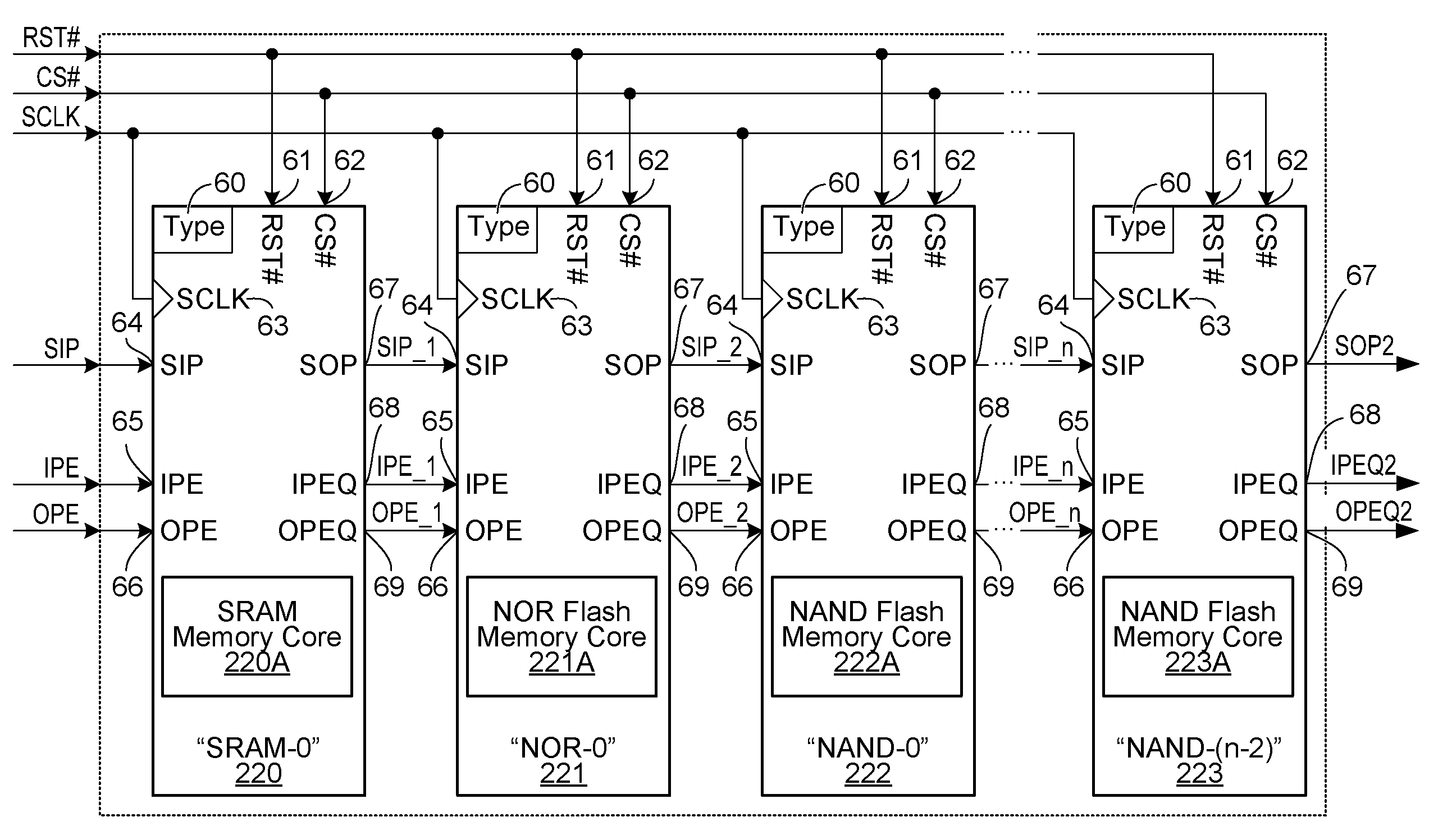
[0066]In the following detailed description of sample embodiments of the invention, reference is made to the accompanying drawings, which form a part hereof, and in which is shown by way of illustration specific sample embodiments in which the present invention may be practiced. These embodiments are described in sufficient detail to enable those skilled in the art to practice the present invention, and it is to be understood that other embodiments may be utilized and that logical, mechanical, electrical, and other changes may be made without departing from the scope of the present invention. The following detailed description is, therefore, not to be taken in a limiting sense, and the scope of the present invention is defined by the appended claims.

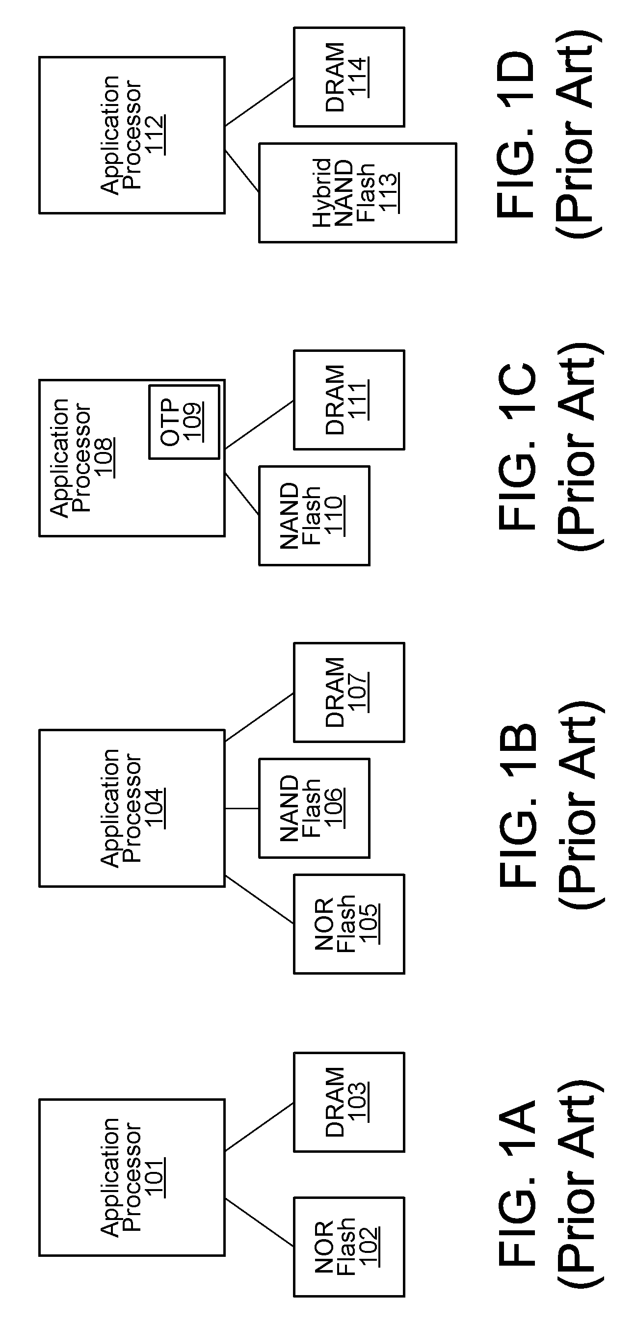
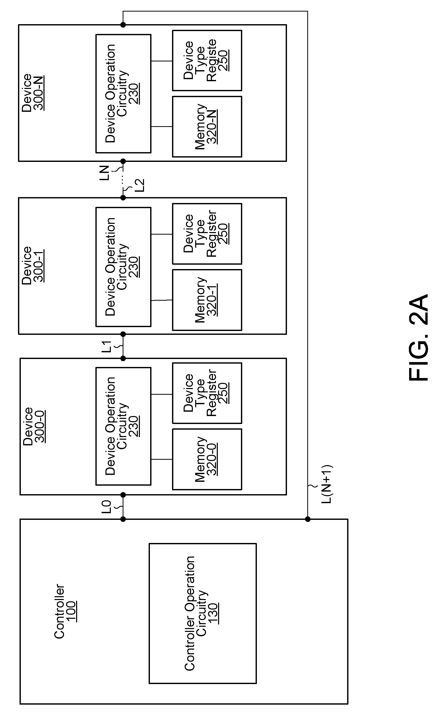
[0067]Generally, the present invention provides apparatus and method for controlling semiconductor devices, such as, for example, memory systems with memory devices of mixed type.

[0068]Embodiments of the present invention are now describ...


PUM


Abstract

A memory system architecture is provided in which a memory controller controls memory devices in a serial interconnection configuration. The memory controller has an output port for sending memory commands and an input port for receiving memory responses for those memory commands requisitioning such responses. Each memory device includes a memory, such as, for example, NAND-type flash memory, NOR-type flash memory, random access memory and static random access memory. Each memory command is specific to the memory type of a target memory device. A data path for the memory commands and the memory responses is provided by the interconnection. A given memory command traverses memory devices in order to reach its intended memory device of the serial interconnection configuration. Upon its receipt, the intended memory device executes the given memory command and, if appropriate, sends a memory response to a next memory device. The memory response is transferred to the memory controller.

Description

CROSS REFERENCE TO RELATED APPLICATIONS[0001]This application claims the benefits of U.S. Provisional Patent Application No. 60 / 868,773 filed Dec. 6, 2006; U.S. Provisional Patent Application No. 60 / 870,892 filed Dec. 20, 2006; and U.S. patent application Ser. No. 11 / 622,828 filed Jan. 12, 2007, the disclosures of which are expressly incorporated herein by reference in their entirety.FIELD OF THE INVENTION[0002]The present invention relates generally to semiconductor device systems. More particularly, the present invention relates to an apparatus and a method for controlling semiconductor devices, such as, for example, memory systems with memory devices of varying or mixed type.BACKGROUND OF THE INVENTION[0003]Computer-based systems contain semiconductor devices, such as, for example, memory devices and processing devices. Memory is where information is stored while waiting to be operated on by the Central Processing Unit (CPU) of the computer. Memory is controlled by a memory contr...

Claims


Application Information

Patent Timeline
Patent Type & Authority Applications(United States)
IPC IPC(8): G06F12/02
CPCG06F13/4239G11C2216/30G11C16/20G11C16/08
Inventor OH, HAKJUNEPYEON, HONG BEOMKIM, JIN-KI
Owner CONVERSANT INTPROP MANAGEMENT INC
Why Eureka
Try Eureka