
Heteroacene compound, organic thin film comprising the compound, and electronic device comprising the thin film

a technology of heteroacene compound and organic thin film, applied in the field of heteroacene compound, can solve the problems of increasing off-state leakage current, increasing charge mobility, and requiring a relatively expensive vacuum deposition apparatus, and achieves the effect of improving processability and increasing charge mobility

Active Publication Date: 2008-06-19
SAMSUNG ELECTRONICS CO LTD
View PDF2 Cites 39 Cited by
  • Summary
  • Abstract
  • Description
  • Claims
  • Application Information

AI Technical Summary

Benefits of technology

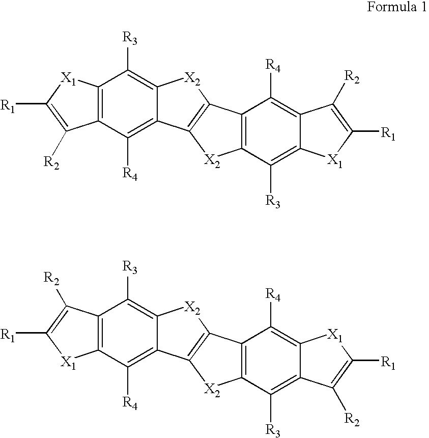
[0008]Accordingly, example embodiments have been made keeping in mind the above problems occurring in the related art, and example embodiments provide a low-molecular-weight heteroacene compound, which may have a compact planar structure in which all six rings may be fused together, thereby exhibiting increased charge mobility, and furthermore, enabling the use of a deposition process or a room-temperature solution process when applied to devices, therefore realizing improved processability.

Problems solved by technology

However, problems of decreased charge mobility and increased off-state leakage current may be caused.
Further, low-molecular-weight organic material, e.g., pentacene, may have increased charge mobility of about 3.2˜5.0 cm2 / Vs or more, but may require a relatively expensive apparatus for vacuum deposition at the time of forming a thin film.
Therefore, the low-molecular-weight organic material may be unsuitable for use in the preparation of a film having a relatively large area, and processability may be undesirable.

Method used


Image

  • Heteroacene compound, organic thin film comprising the compound, and electronic device comprising the thin film
  • Heteroacene compound, organic thin film comprising the compound, and electronic device comprising the thin film
  • Heteroacene compound, organic thin film comprising the compound, and electronic device comprising the thin film

Examples


example 3

PREPARATIVE EXAMPLE 3

[0076]

[0077]The desired compound 12 was synthesized in the same manner as in Preparative Example 2, with the exception that 2-heptylcarbonylthiophene was used instead of 2-octyl-5-formyl thiophene.

[0078]NMR (CDCl3) 7.75 (d, 2H), 7.57 (d, 2H), 7.43 (s, 2H), 2.70 (t, 4H), 1.75 (m, 4H), 1.60 (m, 4H), 1.34 (m, 8H), 0.95 (t, 6H); GC-MS (M+) 547.

example 4

PREPARATIVE EXAMPLE 4

[0079]

[0080]The desired compound 15 was synthesized in the same manner as in Preparative Example 3, with the exception that 3-heptylcarbonylthiophene was used instead of 2-heptylcarbonylthiophene.

[0081]NMR (CDCl3) 7.80 (d, 2H), 7.60(d, 2H), 7.49 (s, 2H) 2.68 (t, 4H), 1.74 (m, 4H), 1.58 (m, 4H), 1.32 (m, 8H), 0.90 (t, 6H); GC-MS (M+) 547.

[Fabrication of Organic Thin Film Transistor]

example 1

[0082]On a washed glass substrate, aluminum (Al) for a gate electrode was deposited to a thickness of about 1000 Å through sputtering, and then organic and inorganic hybrid insulating material was applied through spin casting and dried at about 200° C. for about 2 hours, thus forming a gate insulating layer about 7000 Å thick. Subsequently, gold (Au) for source / drain electrodes was deposited thereon to a thickness of about 700 Å through thermal evaporation. Thereafter, the compound synthesized in Preparative Example 1 was deposited to a thickness of about 700 Å through thermal evaporation to thus prepare an organic semiconductor layer, thereby fabricating an organic thin film transistor (OTFT).


PUM


Abstract

A heteroacene compound includes a di-thieno-benzo-thieno-thiophene derivative, in which all six rings may be fused together, an organic thin film including the same, and an electronic device that includes the thin film as a carrier transport layer. The compound of example embodiments may have a compact planar structure to thus realize improved solvent solubility and processability. When the compound is applied to electronic devices, a deposition process or a room-temperature solution process may be applied, and as well, intermolecular packing and stacking may be efficiently realized, resulting in improved electrical properties, including increased charge mobility.

Description

PRIORITY STATEMENT[0001]This non-provisional application claims priority under U.S.C. § 119 to Korean Patent Application No. 2006-126931, filed on Dec. 13, 2006, in the Korean Intellectual Property Office (KIPO), the entire contents of which are incorporated herein by reference.BACKGROUND[0002]1. Field[0003]Example embodiments relate to a heteroacene compound and applications thereof. Other example embodiments relate to a heteroacene compound, in which all six rings may be fused together, an organic thin film comprising the compound, an electronic device comprising the thin film as a carrier transport layer and methods of fabricating the organic thin film and the electronic device.[0004]2. Description of the Related Art[0005]In general, flat display devices, e.g., liquid crystal displays or organic electroluminescent displays, are provided with a variety of thin film transistors (TFTs) to drive them. The TFT may include a gate electrode, source / drain electrodes, and a semiconductor ...

Claims


Application Information

Patent Timeline
IPC IPC(8): C07D409/14H01L29/08
CPCH01L51/0074H01L51/0508C07D495/22C09K19/3491Y02E10/549C09K19/40C09K2019/3408H01L51/0056C09K19/3494H10K85/624H10K85/6576H10K10/46H10K99/00H10K10/00
Inventor PARK, JONG ILJEONG, EUN JEONGLEE, SANG YOONLEE, BANG LINHAN, KOOK MIN
Owner SAMSUNG ELECTRONICS CO LTD
Learn More