

Three dimensional image display and manufacturing method thereof
- Summary
- Abstract
- Description
- Claims
- Application Information
AI Technical Summary
Benefits of technology
Problems solved by technology
Method used
Image

Examples
third embodiment
[0033]FIG. 9 is a view illustrating a structure that a patterned retarder and a wire grid polarizer are adapted to a color filter (C / F) of a TFT-LCD according to the present invention, FIG. 10 is a view illustrating a structure of a TFT glass substrate in which a TFT is formed, FIG. 11 is a view illustrating a state that a light passed through a patterned wire grid polarizer and λ / 2 patterned retarder is linearly polarized, FIG. 12 is a view illustrating a structure according to the present invention, and FIG. 13 is a view illustrating a basic structure of a TFT which is used for a TFT-LCD and an AMOLED.
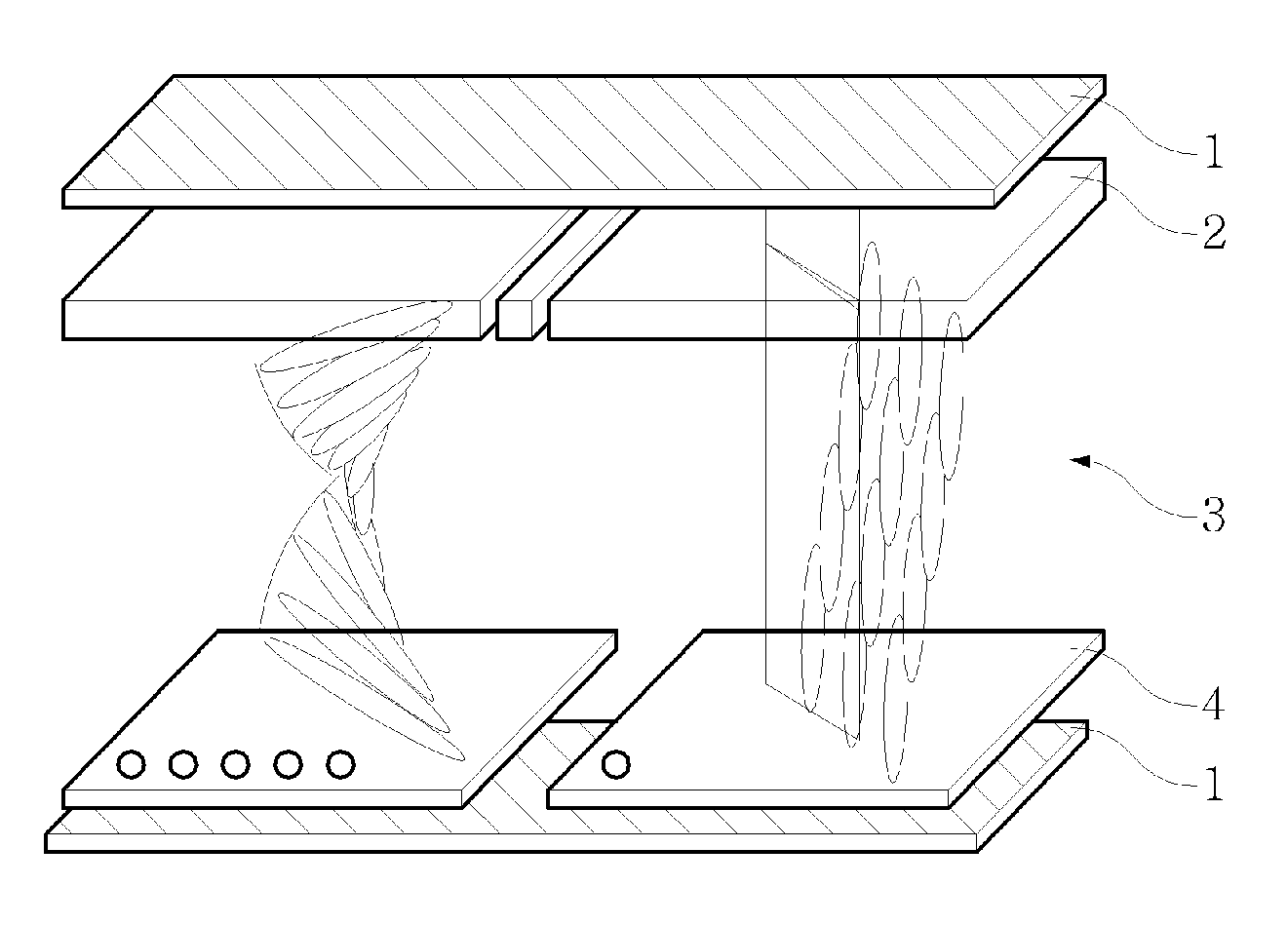
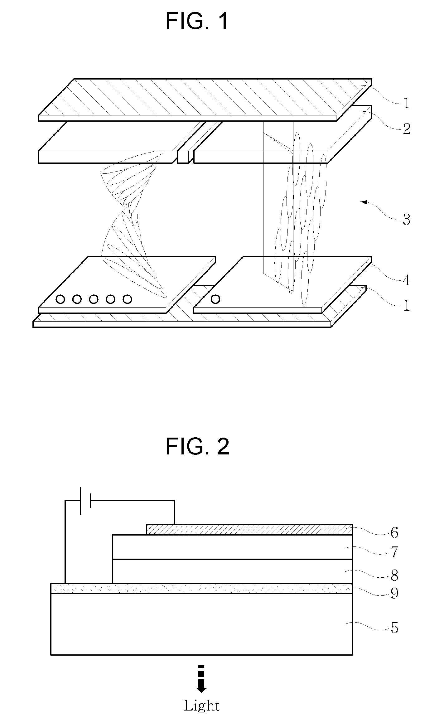
[0034]FIG. 1 is a view illustrating a TFT-LCD. Here, the TFT is a switching device which uses an amorphous silicon as an active layer and is adapted to an active matrix liquid crystal display, a switching device of an electric light emitting device and a peripheral circuit. Generally, an active layer of a thin film transistor used as a switching device for driving a pixel electrode o...
first embodiment
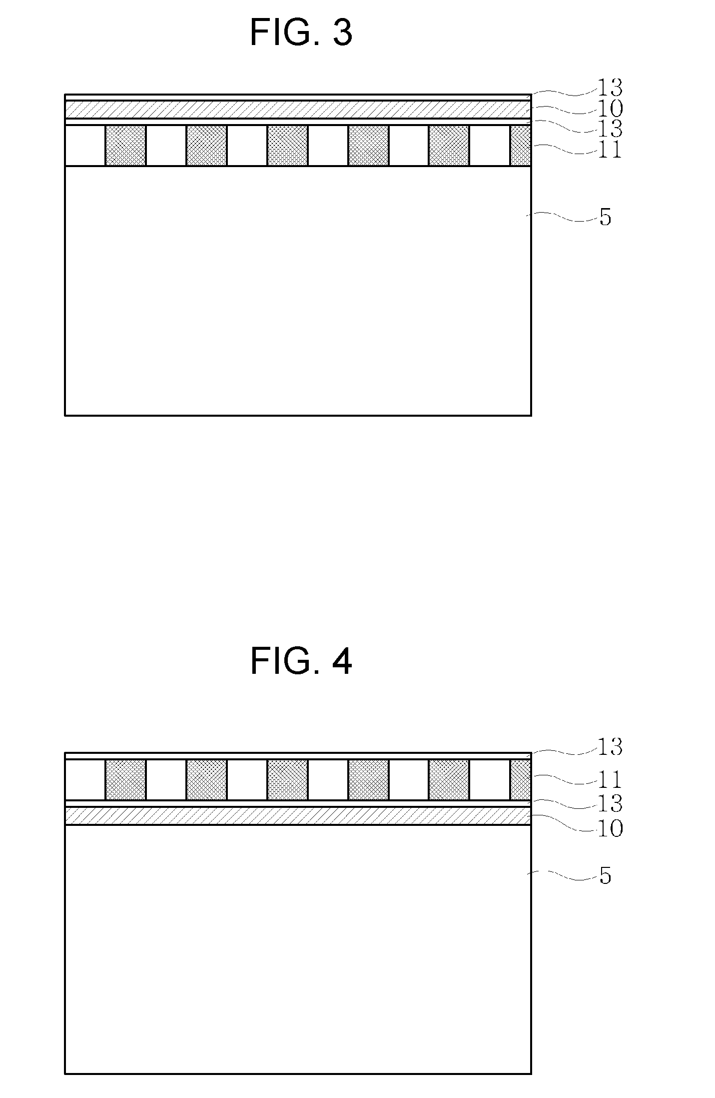
[0038]FIG. 3 is a view illustrating a structure according to the present invention.
[0039]As shown in FIG. 3, a patterned retarder 11 is formed on the glass substrate 5, and a layer of protective coating 13 is formed so as to protect the patterned retarder 111 during the following processes. A wire grid polarizer 10, which micro-patterns a formed metallic thin film, and a layer of protective coating 13 for protecting the wire grid polarizer 10 are sequentially formed. As shown in FIG. 12, the above resultant structure is adapted to a substrate of the color filter plate of the upper part of the TFT-LCD, so that a display can be obtained, which does not have any limitations to a visual distance or a visual angle.
[0040]As shown in FIG. 12, the light from a backlight transmits the polarizer 1, the TFT, the liquid crystal layer 3 and the color filter 2 and then transmits the wire grid polarizer 10 and becomes a linearly polarized light. The light transmits the patterned retarder 11. The p...
second embodiment
[0041]FIG. 4 is a view illustrating a structure according to the present invention.
[0042]As shown in FIG. 4, a wire grid polarizer 10, which micro-patterns a metallic thin film, and a layer of protective coating 13 for protecting the wire grid polarizer 10 are sequentially formed on a glass substrate 5. The patterned retarder 11 is formed, and the layer of protective coating 13 is formed for protecting the patterned retarder 11. FIG. 4 is a view illustrating a structure formed in a sequence reverse to the sequence of the structure of FIG. 3. The above structure is used for the TFT plate in the TFT-LCD structure, and a zigzag type polarizer is used for the substrate of the color filter corresponding to the upper plate, so that the display according to the present invention is obtained without any limitations to a visual distance and a visual angle.
[0043]FIG. 5 is an image illustrating a state that a polarized light is observed by a left eye when a polarizer is used after the polarize...
PUM
 Abstract
Description
Claims
Application Information