Semiconductor device and driving method thereof

a driving method and semiconductor technology, applied in the direction of static indicating devices, organic semiconductor devices, instruments, etc., can solve the problems of easy variation of transistors, inability of mos transistors to function as storage capacitors, and inability to achieve the effect of reducing luminance variations of light-emitting elements and improving image quality of display devices

Inactive Publication Date: 2008-06-19
SEMICON ENERGY LAB CO LTD
View PDF30 Cites 88 Cited by
  • Summary
  • Abstract
  • Description
  • Claims
  • Application Information

AI Technical Summary

Benefits of technology

[0054]By using the present invention, variations of the current value which are caused by variations in the threshold voltage of a transistor can be suppressed. Therefore, desired current can be supplied to a load such as a light-emitting element. In particular, in the case of using a light-emitting element as a load, current supplied to the light-emitting element is determined without depending on the threshold voltage of a transistor because variations in the threshold voltage of the transistor can be compensated in a display device of the present invention. Thus, variations in luminance of the light-emitting element can be reduced, so that image quality of the display device can be improved.

Problems solved by technology

However, electrical characteristics such as the threshold voltage, on current, and mobility of a polysilicon transistor easily vary due to a defect in a crystal grain boundary.
Therefore, the MOS transistor cannot function as a storage capacitor.
Accordingly, video signals cannot be accurately held.

Method used


Image

  • Semiconductor device and driving method thereof
  • Semiconductor device and driving method thereof
  • Semiconductor device and driving method thereof

Examples


embodiment mode 1

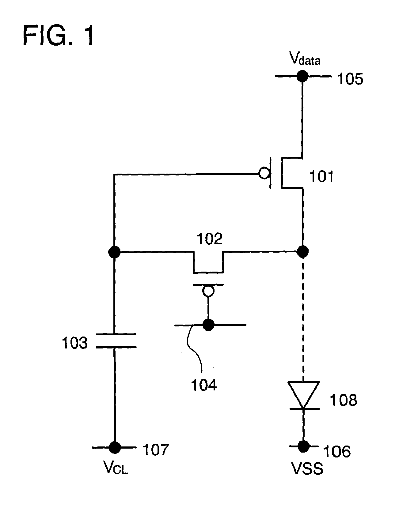
[0124]First, a basic structure of a pixel circuit in a display device of the present invention is described with reference to FIGS. 1 and 2. Note that an EL element is described as an example of a light-emitting element.

[0125]FIG. 1 is a diagram showing a circuit structure for acquiring voltage which is based on video signal voltage and the threshold voltage of a transistor in a pixel structure of this embodiment mode. FIG. 1 shows a circuit including a first transistor 101, a second transistor 102, a storage capacitor 103, a scan line 104, a signal line 105, a power supply line 106, a capacitor line 107, and a light-emitting element 108.

[0126]Note that in FIG. 1, the first transistor 101 and the second transistor 102 are P-channel transistors.

[0127]A gate electrode of the first transistor 101 is connected to a second electrode of the second transistor 102 and a first electrode of the storage capacitor 103; a first electrode of the first transistor 101 is connected to the signal lin...

embodiment mode 2

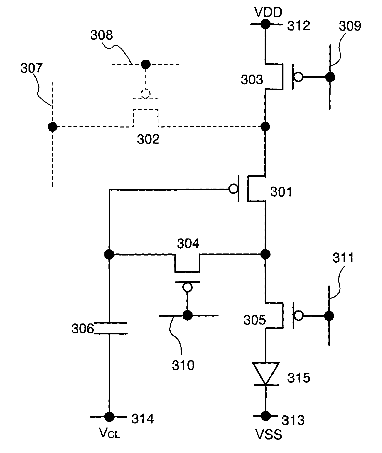
[0214]Although a capacitor line is separately provided in Embodiment Mode 1, another wiring which has been already provided may be used instead of the capacitor line. For example, by using any one of first to fourth scan lines included in a pixel of another row instead of the capacitor line, a capacitor line included in the pixel can be omitted. In this embodiment mode, the case is described in which any one of first to fourth scan lines included in a pixel of another row is used instead of the capacitor line included in the pixel. Note that an EL element is described as an example of a light-emitting element.

[0215]For example, FIG. 21 shows an example of a pixel circuit in the case where a second scan line included in a pixel of a previous row is used instead of a capacitor line included in the pixel in the pixel circuit shown in FIG. 3.

[0216]FIG. 21 shows structures of a Pixel (i) in an i-th row and a Pixel (i−1) in an (i−1)th row, which is a previous row. The Pixel (i−1) in the (...

embodiment mode 3

[0237]Although current is supplied to a light-emitting element when initialization is performed in Embodiment Mode 1 and Embodiment Mode 2, initialization can also be performed by adding an initialization transistor which turns on in a first period T1 to the pixel circuit which is shown heretofore. In this embodiment mode, a method of performing initialization using an initialization transistor is described. Note that an EL element is described as an example of a light-emitting element.

[0238]In order to perform initialization, a second electrode of a first transistor is necessary to be set at an initial potential. At this time, by connecting the second electrode of the first transistor to an electrode of another element or to another wiring through an initialization transistor and turning on the initialization transistor, the second electrode of the first transistor can be set at a potential of the electrode of another element or of another wiring, to which the second electrode of t...


PUM


Abstract

A display device which can compensate for variations of the threshold voltage of transistors and suppress variations in luminance, and a driving method thereof are provided. Current is supplied to a light emitting element and light is emitted from the light emitting element by following steps: in the first period initial voltage is stored in a storage capacitor; in the second period, voltage based on video signal voltage and the threshold voltage of the transistor is stored in the storage capacitor; and in the third period, the voltage stored in the storage capacitor in the second period is applied to a gate electrode of the transistor. By these operation processes, the current which compensates the effect of the variations of the threshold voltage of the transistor can be supplied to the light emitting element. Therefore, variations in luminance are suppressed.

Description

BACKGROUND OF THE INVENTION[0001]1. Field of the Invention[0002]The present invention relates to a structure and a driving method of a semiconductor device having a transistor. In addition, the present invention relates to a structure and a driving method of an active matrix display device using a semiconductor device having a thin film transistor. Further, the present invention relates to an electronic device using such a semiconductor device in a display portion.[0003]2. Description of the Related Art[0004]In recent years, a so-called self-luminous display device having a pixel formed by using a light-emitting element such as a light-emitting diode has attracted attention. As a light-emitting element used for such a self-luminous display device, an organic light-emitting diode (also referred to as an OLED (organic light-emitting diode), an organic EL element, an electroluminescence (electro luminescence: EL) element, and the like) has attracted attention, and it has been used for ...

Claims


Application Information

Patent Timeline
Patent Type & Authority Applications(United States)
IPC IPC(8): G09G3/30
CPCG09G3/3233G09G2300/0819G09G2300/0842G09G2300/0861H01L2251/5323G09G2320/043H01L27/3265H01L2251/5315G09G2310/0262H10K59/1216H10K2102/3031H10K2102/3026G09G3/30H05B33/12G09G3/32G09G3/20
Inventor SHISHIDO, HIDEAKI
Owner SEMICON ENERGY LAB CO LTD
Why Eureka
Try Eureka