Pet-based touch pad

a technology of touch pad and pet, which is applied in the direction of dielectric characteristics, instruments, wireless commuication services, etc., can solve the problem of widened sensor panels, and achieve the effect of more flexibility in product design

Active Publication Date: 2008-06-19
APPLE INC
View PDF32 Cites 210 Cited by
  • Summary
  • Abstract
  • Description
  • Claims
  • Application Information

AI Technical Summary

Benefits of technology

[0009]To establish off-panel connections with the rows, metal traces can be connected to the rows and routed along the borders of the bottom PET layer to the first tail. In some embodiments, traces can also be connected to rows and routed along the borders of the PET layer to a second tail. To prevent shorts or damage to traces, especially where those traces make right-angled bends, PET coverlay can be applied to the bottom PET layer prior to lamination with the other layers in the stack.
[0010]The tails can be integrally formed with the PET layer, and can be directly inserted into connectors such as zero insertion force (ZIF) connectors on a system board, or in other embodiments flex connectors such as flexible printed circuits (FPCs) can be conductively bonded to the tails. The mutual capacitance design of the sensor panel can enable the use of a second tail or flex circuits to connect to remote components, because the parasitic capacitance inherent in long connectors does not have a direct effect on the sensed signaling appearing on the column traces leaving the sensor panel. In contrast, self-capacitance sensor panels can be very susceptible to parasitic capacitance, and thus usually require very short connectors. Thus, in general, mutual capacitance touch sensor panels can allow more flexibility in product design, and can allow the sensor panel to be remotely located from other system components.

Problems solved by technology

For example, because it can be more difficult to form thin metal traces on plastic substrates, sensor panels formed with metal traces on the borders can force the sensor panel to be widened.

Method used


Image

  • Pet-based touch pad
  • Pet-based touch pad
  • Pet-based touch pad

Examples


Embodiment Construction

[0019]In the following description of preferred embodiments, reference is made to the accompanying drawings which form a part hereof, and in which it is shown by way of illustration specific embodiments in which the invention may be practiced. It is to be understood that other embodiments may be utilized and structural changes may be made without departing from the scope of the preferred embodiments of the present invention.

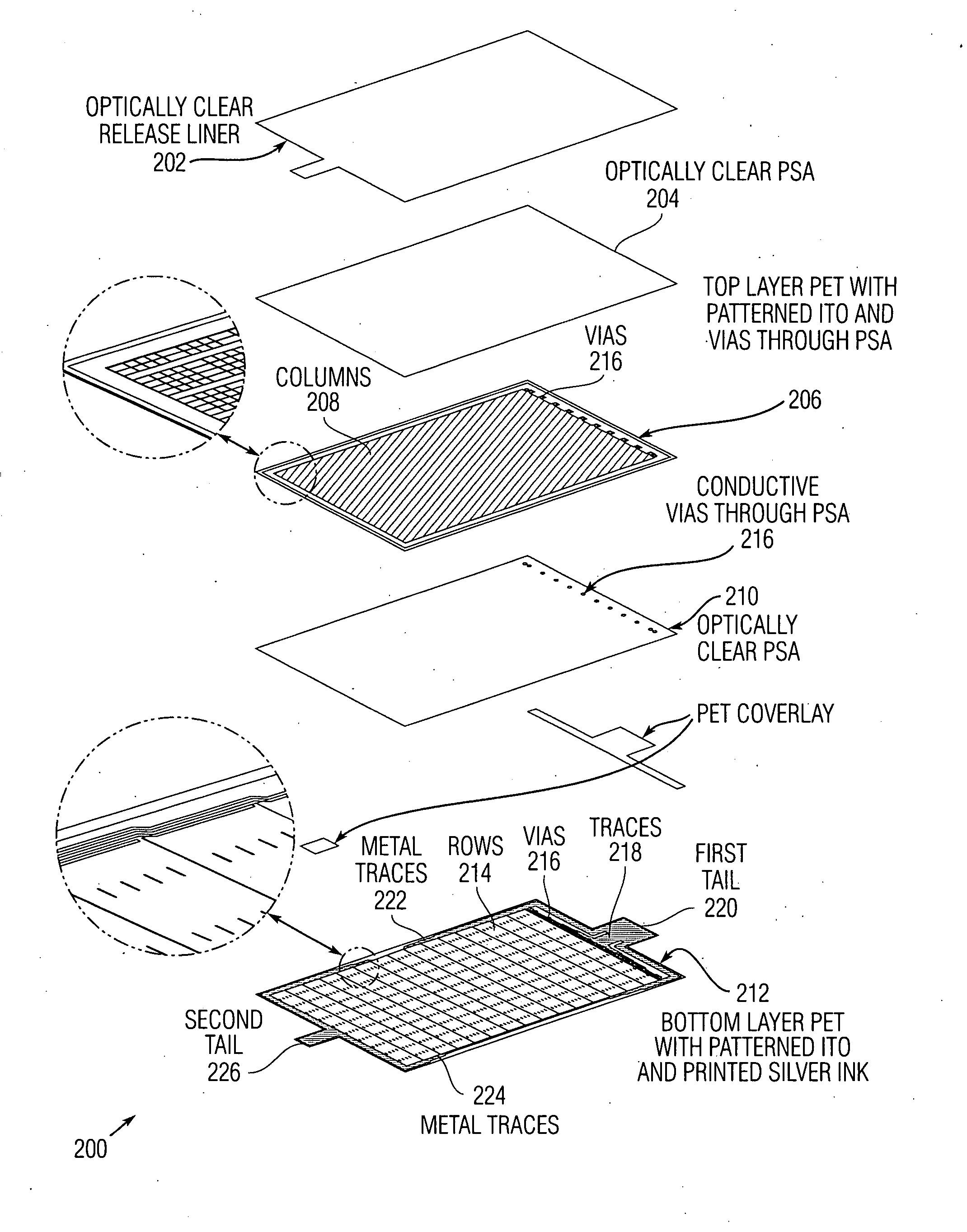
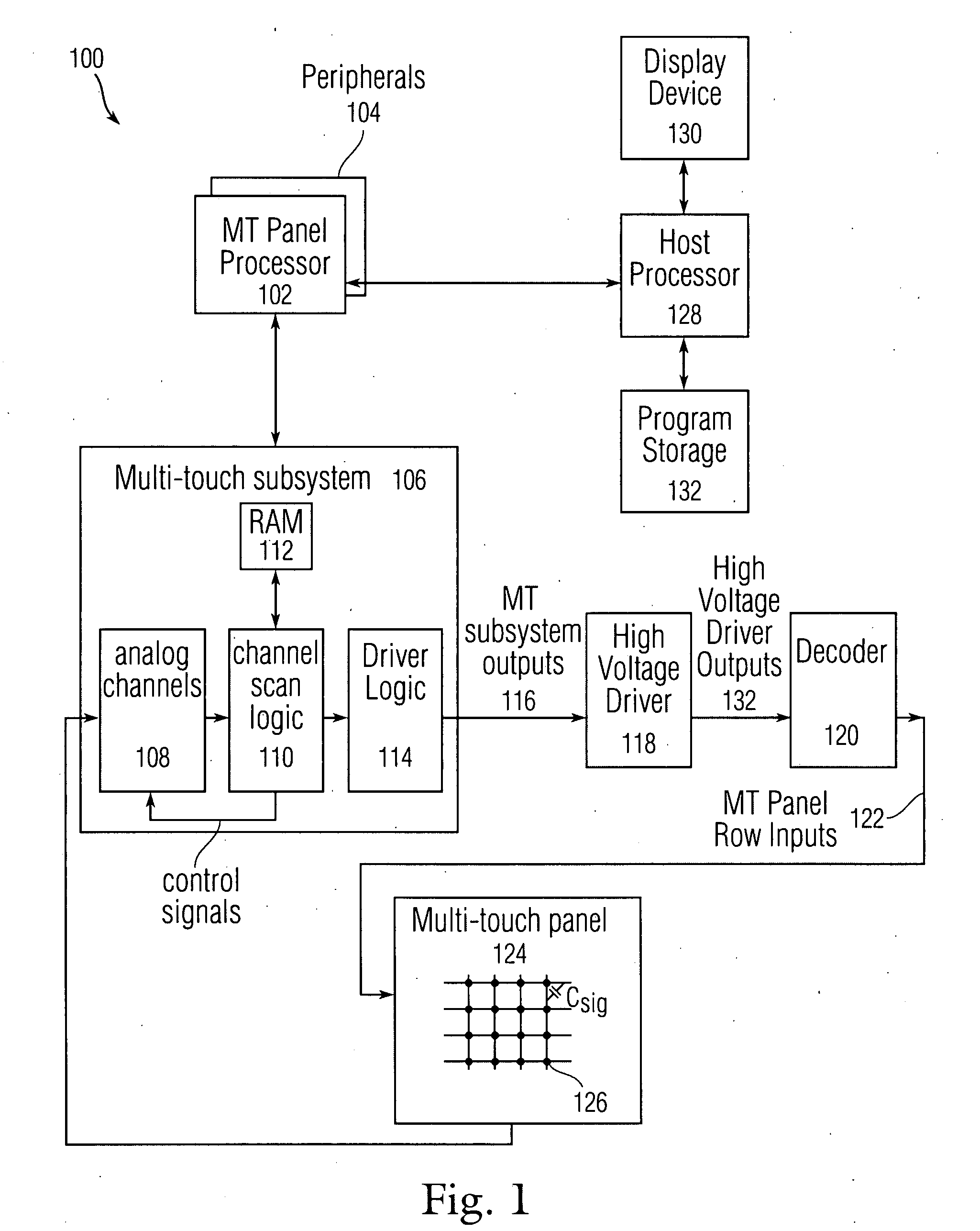
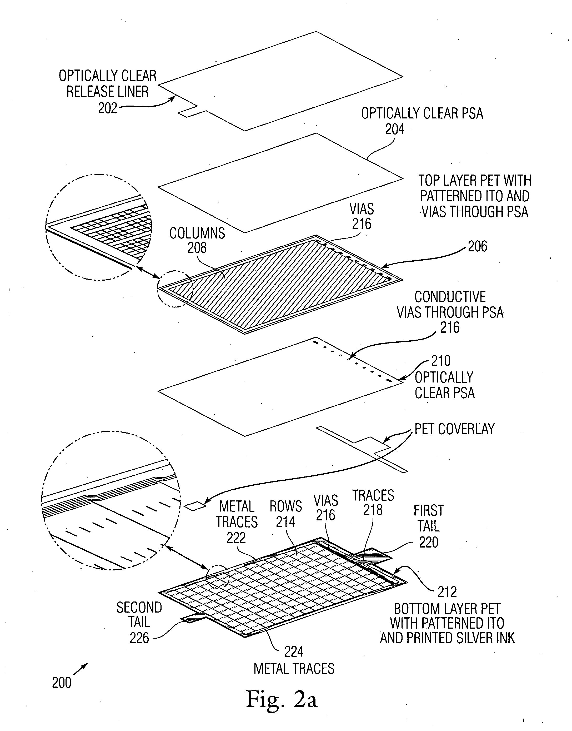
[0020]A substantially transparent sensor panel can be formed using plastic substrates to take advantage of the cost-effectiveness and manufacturing ease of plastic. Although some capacitive sensor panels can employ rows and columns formed on opposite sides of the same substrate, this approach can be difficult when using plastic substrates. Therefore, in embodiments of the invention, rows and columns can be formed on separate first and second substrates formed from a plastic such as PET.

[0021]In particular, a space-efficient substantially transparent mutual capaci...


PUM

PropertyMeasurementUnit
transparentaaaaaaaaaa
transparent conductiveaaaaaaaaaa
mutual capacitanceaaaaaaaaaa

Abstract

A space-efficient substantially transparent mutual capacitance touch sensor panel can be created by forming columns made of a substantially transparent conductive material on one side of a first substantially transparent substrate, forming rows made of the substantially transparent conductive material on one side of a second substantially transparent substrate, adhering the two substrates together with a substantially transparent adhesive, bringing column connections down to the second substrate using vias, and routing both the column and row connections to a single connection area on the second substrate. In addition, in some embodiments some of the row connections can be routed to a second connection area on the second substrate to minimize the size of the sensor panel.

Description

CROSS-REFERENCE TO RELATED APPLICATIONS[0001]The present invention claims the benefit under 35 USC 119(e) of U.S. provisional patent application Ser. No. 60 / 875,037 filed Dec. 15, 2006, the contents of which are incorporated by reference herein.FIELD OF THE INVENTION[0002]This invention relates to touch sensor panels, and more particularly, to substantially transparent mutual capacitance touch sensor panels having rows and columns formed on separate plastic substrates.BACKGROUND OF THE INVENTION[0003]Many types of input devices are presently available for performing operations in a computing system, such as buttons or keys, mice, trackballs, touch panels, joysticks, touch screens and the like. Touch screens, in particular, are becoming increasingly popular because of their ease and versatility of operation as well as their declining price. Touch screens can include a touch panel, which can be a clear panel with a touch-sensitive surface. The touch panel can be positioned in front of...

Claims


Application Information

Patent Timeline
Patent Type & Authority Applications(United States)
IPC IPC(8): G06F3/041
CPCG06F3/0416Y10T29/49165G06F2203/04107G06F3/044G06F3/04164G06F3/04166G06F3/0445G06F3/0446G06F3/047G06F2203/04103G06F2203/04104H05K1/0353H05K1/11H05K3/10H05K2201/0108H05K2201/0326
Inventor HOTELLING, STEVE PORTER
Owner APPLE INC
Why Eureka
Try Eureka