Method for manufacturing a semiconductor device

a manufacturing method and semiconductor technology, applied in semiconductor devices, semiconductor/solid-state device testing/measurement, instruments, etc., can solve the problem of complicated configuration of element regions from a plain view, and achieve the effect of reducing the variation of area and configuration of soi layers, reducing misalignment of locations, and reducing the fluctuation of area and configuration

Inactive Publication Date: 2008-06-19
SEIKO EPSON CORP
View PDF5 Cites 5 Cited by
  • Summary
  • Abstract
  • Description
  • Claims
  • Application Information

AI Technical Summary

Benefits of technology

[0008]An advantage of the present invention is to provide a method of manufacturing a semiconductor device to overcome the above issue newly revealed as development of the SBSI method. The method is able to reduce variation of area and configuration of a SOI layer when the SOI layer is formed on a semiconductor substrate.
[0009]According to an aspect of the invention, a method of manufacturing a semiconductor device includes: a) depositing a first semiconductor layer and a second semiconductor layer in a semiconductor substrate in series; b) forming a first groove penetrating the first and second semiconductor layers and placed adjacent to an element region by partly etching the first and second semiconductor layers; c) forming a supporting member that supports the second semiconductor layer, covers over the second semiconductor layer and is embedded into the first groove; d) forming a second groove that exposes the first semiconductor layer from the bottom of the second semiconductor layer supported by the supporting member and is placed near the element region; and e) forming a cavity between the semiconductor substrate and the second semiconductor layer in the element region by etching the first semiconductor layer via the second groove under a specific condition in which the first semiconductor layer is easily etched, compared to the second semiconductor layer. Step b) further comprises: forming an alignment mark on the semiconductor substrate while forming the first groove by photolithography and etching for forming the first groove. Step d) further comprises: aligning the position of photolithography by using the alignment mark.
[0010]In the conventional SBSI method, the configuration of a element region was relatively simple and misaligning the second groove (namely a hole for removing SiGe) with the first groove (namely a supporting hole) a little did not affect an area of an element region and its configuration. Hence, the positional relationship between the first groove and the second groove was not paid attention. Therefore, both the first groove and the second groove were aligned while arbitrary patterns in a previous process worked as a mark for them. For example, in manufacturing a hybrid semiconductor device including a SOI structure and a bulk structure, a LOCOS structure for isolating elements in a bulk is worked as a mark for aligning these grooves.
[0011]On the other hand, according to the first aspect of the invention, the first groove and an alignment mark are simultaneously patterned with a same photo mask and the second groove is patterned while this alignment mark works as a mark. Namely, in the process of forming the second groove, the second groove is aligned as the first groove working as a reference, instead of LOCOS, reducing misalignment of location of the second groove to the first location compared to a case in which LOCOS works as a reference. Accordingly, the second semiconductor layer is formed as an element region surrounded by the first and second grooves while reducing fluctuation of its area and configuration.
[0012]According to the aspect of the invention, the first and second grooves may be formed so as to sandwich a region to be a channel in the element region from a plain view. In case when a region to be a channel (also called as a channel region) is sandwiched between the first and second grooves from a plain view, if the position of the second groove is misaligned to that of the first groove, the length of the channel region, namely an actual channel width may be out of the predetermined value. The above method, however, reduces misalignment of the position of the second groove to the first groove, contributing to reduction of fluctuation about the channel width W.
[0013]According to the aspect of the invention, the first and second grooves may be formed and adjacently located together so as to sandwich the element region from a plain view and to overlap the second groove with the end of the first groove at the interface between the first groove and the second groove.

Problems solved by technology

Further, wide application of the SBSI method such as manufacturing SRAM and the like makes the configuration of an element region from a plain view (called as plain configuration) complicated.
However, there recently increases a case in which such misaligning of the positional relationship between the supporting hole h′ and the hole H′ for removing SiGe a little greatly varies an area of an element region and its plain configuration.

Method used


Image

  • Method for manufacturing a semiconductor device
  • Method for manufacturing a semiconductor device
  • Method for manufacturing a semiconductor device

Examples


first embodiment

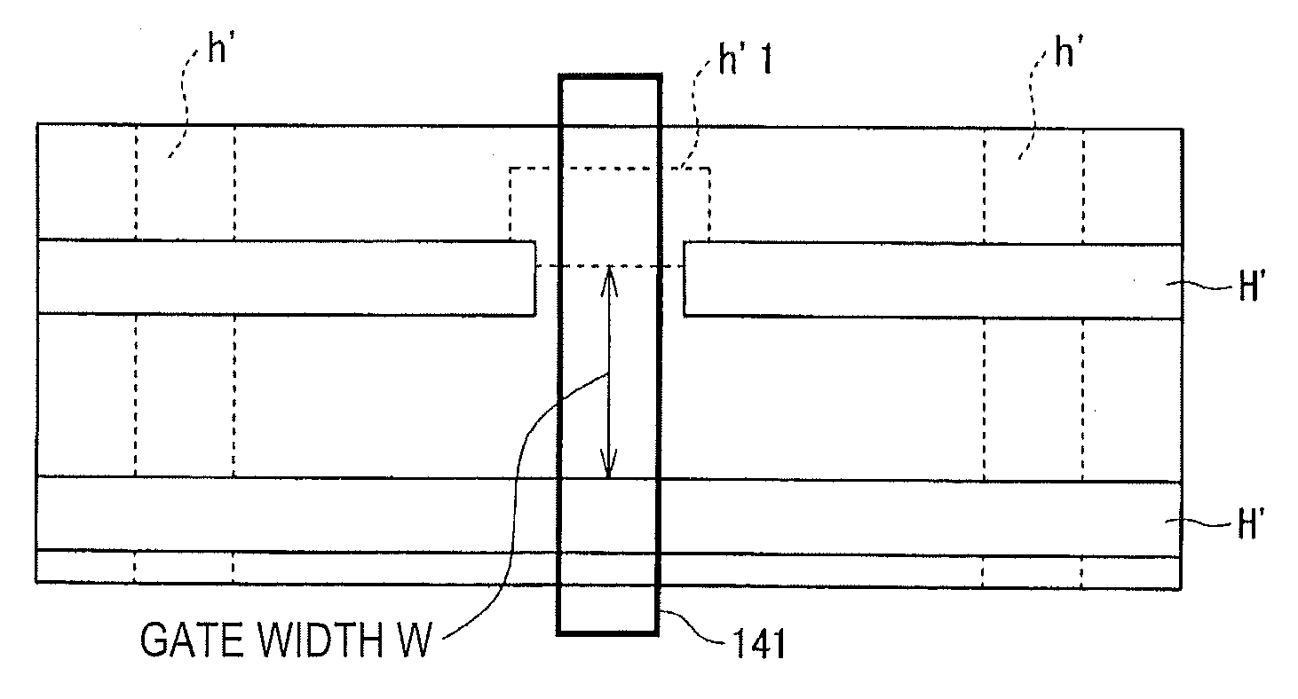
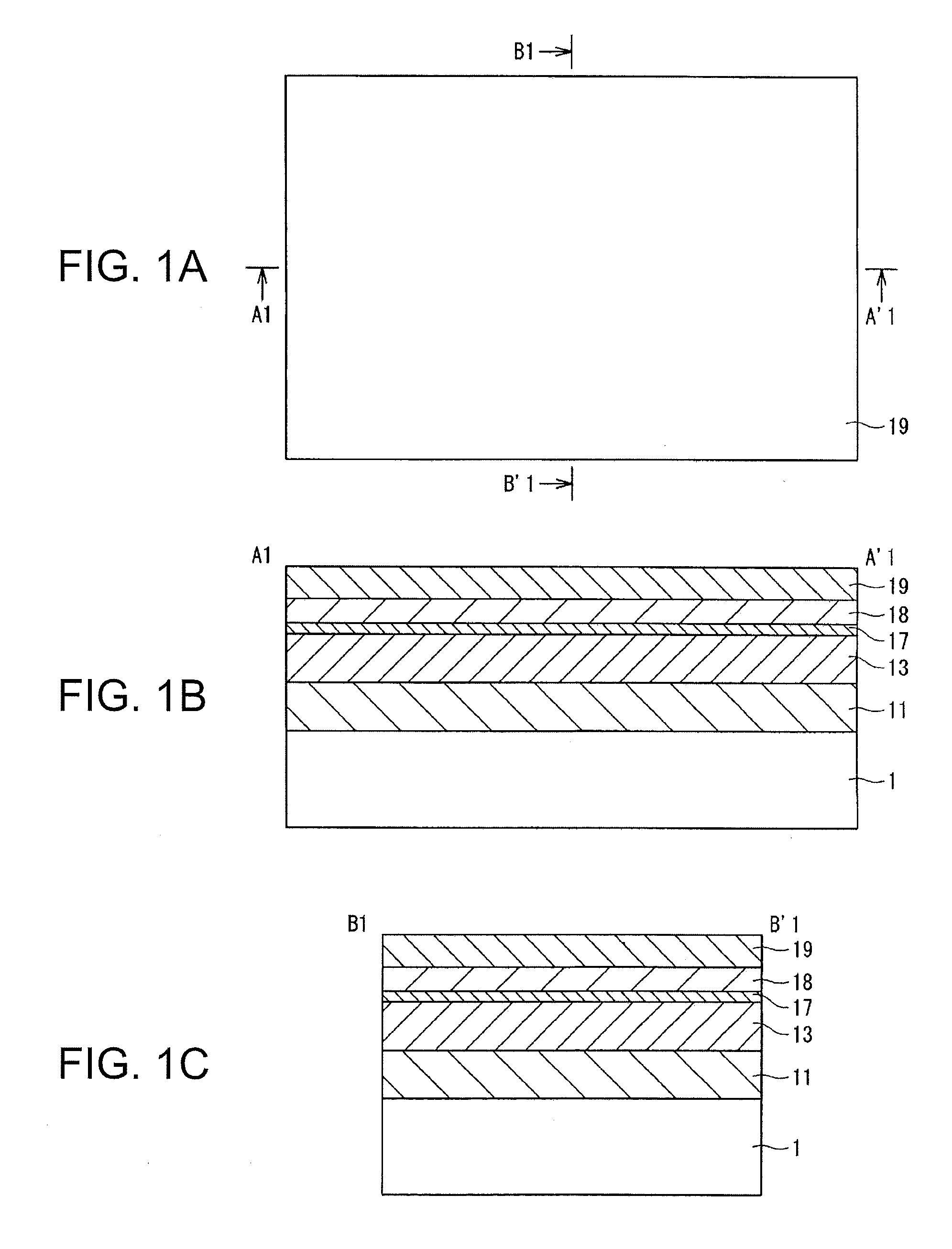
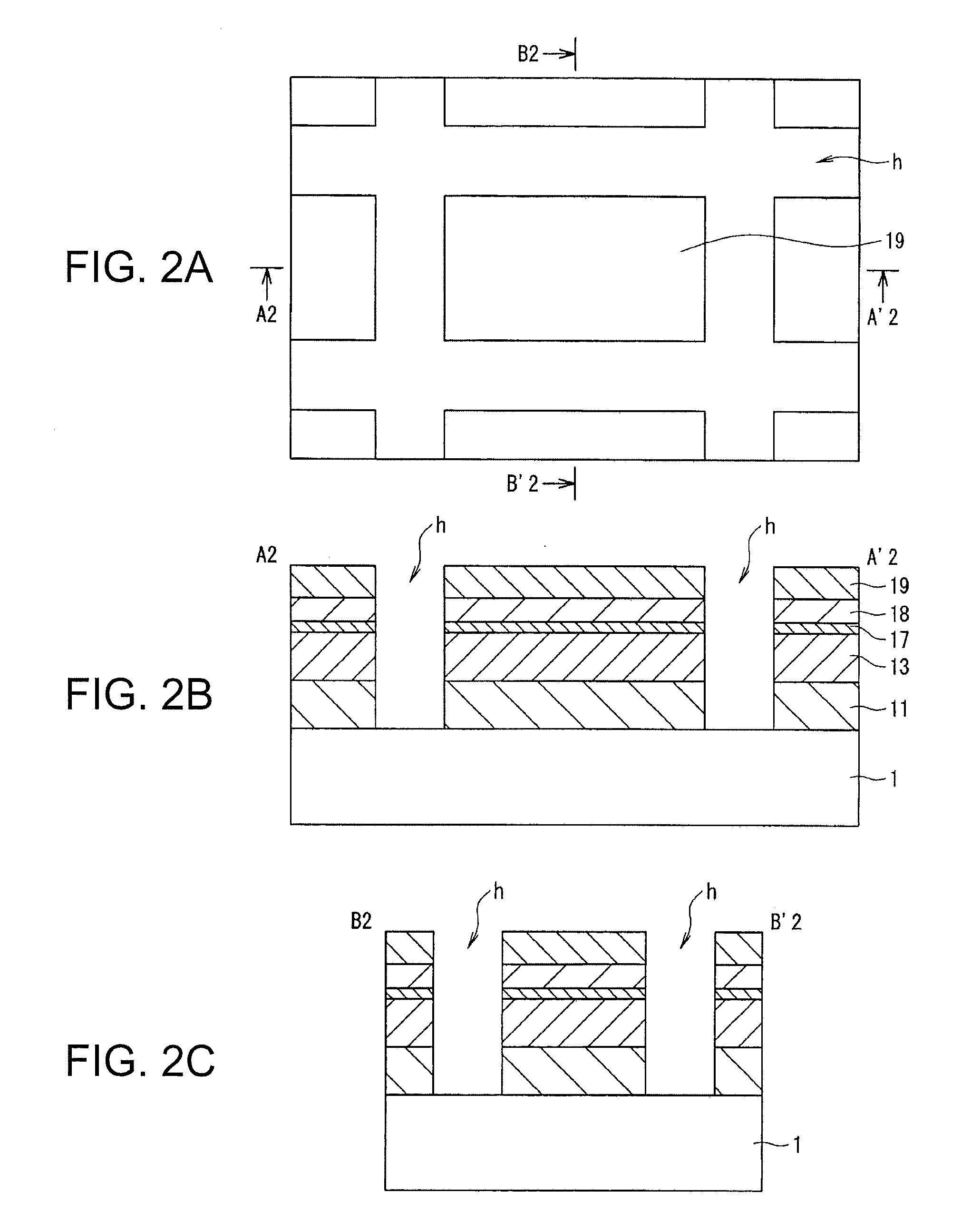
[0034]FIG. 1 to FIG. 9 show a method of manufacturing a semiconductor device of a first embodiment of the invention. FIG. 1A to FIG. 9A are plain views, FIG. 1B to FIG. 9B are cross sections along the lines A1-A1′ to A9-A9′ of FIG. 1A to FIG. 9A, and FIG. 1C to FIG. 9C are cross sections along the lines B1-B1′ to B9-B9′ of FIG. 1C to FIG. 9C.

[0035]First, as shown in FIGS. 1A to 1C, a mono crystalline silicon buffer layer not shown in the figure is formed on a Si substrate 1, then, a mono crystalline silicon germanium (SiGe) layer 11 is formed on it, further, a mono crystalline silicon (Si) layer 13 is formed on it. These Si buffer layer, Si Ge layer 11 and Si layer 13 are continuously grown by an epitaxial growing method, for example. Next, a SiO2 layer 17 is formed on an entire surface of the Si substrate 1, a silicon nitride (Si3 N4) layer 18 is formed on it and further, a SiO2 layer 19 is formed on it. These SiO2 layer 17, (Si3 N4) layer 18 and SiO2 layer 19 are formed by CVD.

[00...


PUM


Abstract

A method of a semiconductor device comprises: a) depositing a first semiconductor layer and a second semiconductor layer in a semiconductor substrate in series; b) forming a first groove penetrating the first and second semiconductor layers and placed adjacent to an element region by partly etching the first and second semiconductor layers; c) forming a supporting member that supports the second semiconductor layer and covers over the second semiconductor layer and is embedded into the first groove; d) forming a second groove that exposes the first semiconductor layer from the bottom of the second semiconductor layer supported by the supporting member and is placed near the element region; and e) forming a cavity between the semiconductor substrate and the second semiconductor layer in the element region by etching the first semiconductor layer via the second groove under a specific condition in which the first semiconductor layer is easily etched, compared to the second semiconductor layer. Step b) further comprises: forming an alignment mark on the semiconductor substrate while forming the first groove by photolithography and etching for forming the first groove. Step d) further comprises aligning the position of photolithography by using the alignment mark.

Description

[0001]The entire disclosure of Japanese Patent Application No. 2006-341645, filed Dec. 19, 2006 is expressly incorporated by reference herein.BACKGROUND OF THE INVENTION[0002]1. Technical Field[0003]Several aspects of the present invention relates to a method of manufacturing a semiconductor device. In particular, it relates to a technology of partly forming a SOI structure on a semiconductor substrate, in which a SOI layer is formed with reducing fluctuation of areas and plain configurations.[0004]2. Related Art[0005]JP-A-2005-354024 and JP-A-2006-41331 disclose this technology and a method of partly forming a SOI structure on a bulk substrate (namely a SBSI method), attaining low cost for forming a SOI transistor. According to the SBSI method, Si and SiGe layers are formed on the Si substrate and a supporting hole h′, which penetrates through Si and SiGe layers and reaches the SI substrate, is formed as shown in FIG. 15A. Next, as shown in FIG. 15B, a supporting film 122 is formed...

Claims


Application Information

Patent Timeline
Patent Type & Authority Applications(United States)
IPC IPC(8): H01L21/76
CPCH01L21/76224H01L22/12H01L22/34H01L2924/0002H01L2924/00G03F9/7046
Inventor KATO, JURI
Owner SEIKO EPSON CORP
Why Eureka
Try Eureka