Semiconductor device and manufacturing method of semiconductor device

a semiconductor and manufacturing method technology, applied in the direction of semiconductor devices, semiconductor/solid-state device details, electrical devices, etc., can solve the problems of long manufacturing process and considerable time and labor, and achieve the effect of high productivity

Active Publication Date: 2008-06-26
FUJI ELECTRIC CO LTD
View PDF11 Cites 27 Cited by
  • Summary
  • Abstract
  • Description
  • Claims
  • Application Information

AI Technical Summary

Benefits of technology

[0018]According to the semiconductor device and the manufacturing method of the semiconductor device described as above, it is possible to achieve a semiconductor

Problems solved by technology

However, because individual wires have to be welded one by one, there arises a problem that the manufacturing process takes too long a time.
Moreover, because the number of wires in

Method used


Image

  • Semiconductor device and manufacturing method of semiconductor device
  • Semiconductor device and manufacturing method of semiconductor device
  • Semiconductor device and manufacturing method of semiconductor device

Examples


Embodiment Construction

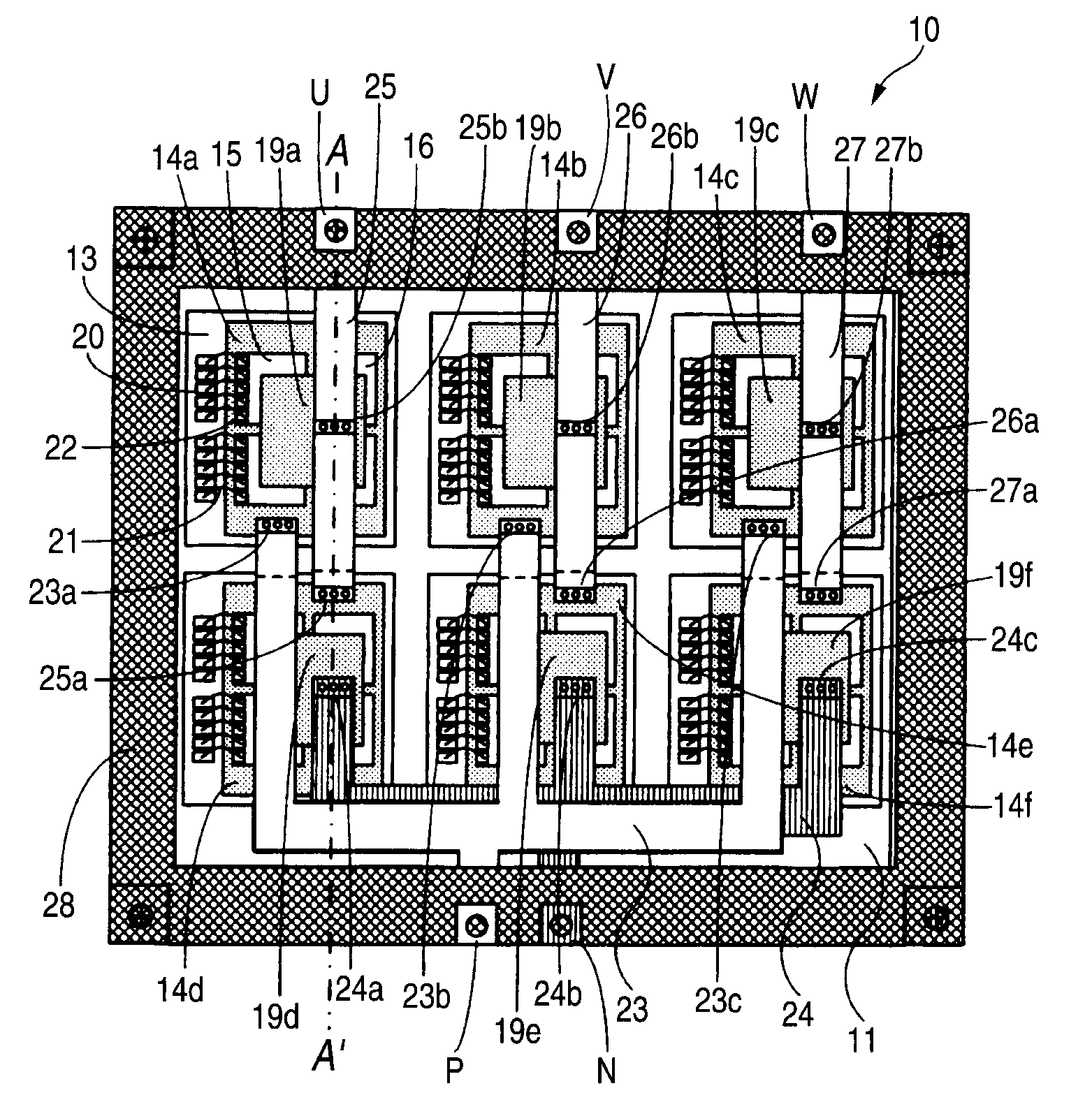
[0036]Hereinafter, one embodiment of the invention will be described in detail with reference to the drawings. In this embodiment, a three-phase inverter incorporating IGBT elements and FWD (Free Wheeling Diode) elements will be described as an example of a semiconductor device.

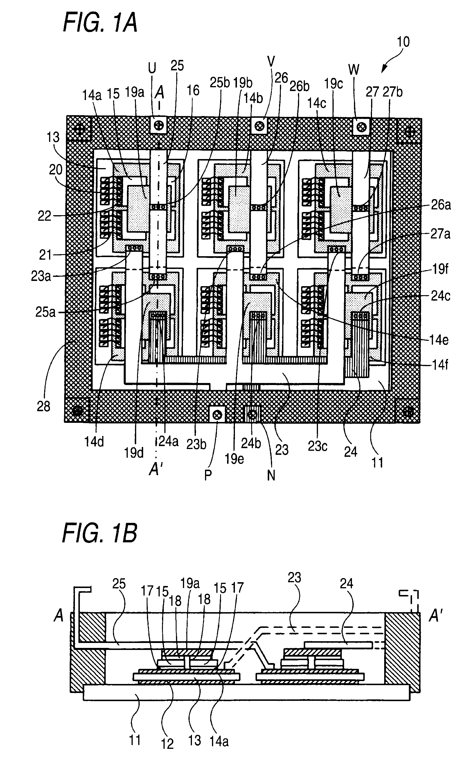
[0037]FIGS. 1A and 1B are schematic views of the major portion of the semiconductor device. FIG. 1A is a schematic top view of the major portion and FIG. 1B is a schematic cross section of the major portion. Herein, FIG. 1B corresponds to the position of the cross section taken along line A-A′ in FIG. 1A. In these drawings, external extraction lead pins for the electrode that are used to control the semiconductor element and provided to a resin case 28 are omitted. The lead pins will be described below.

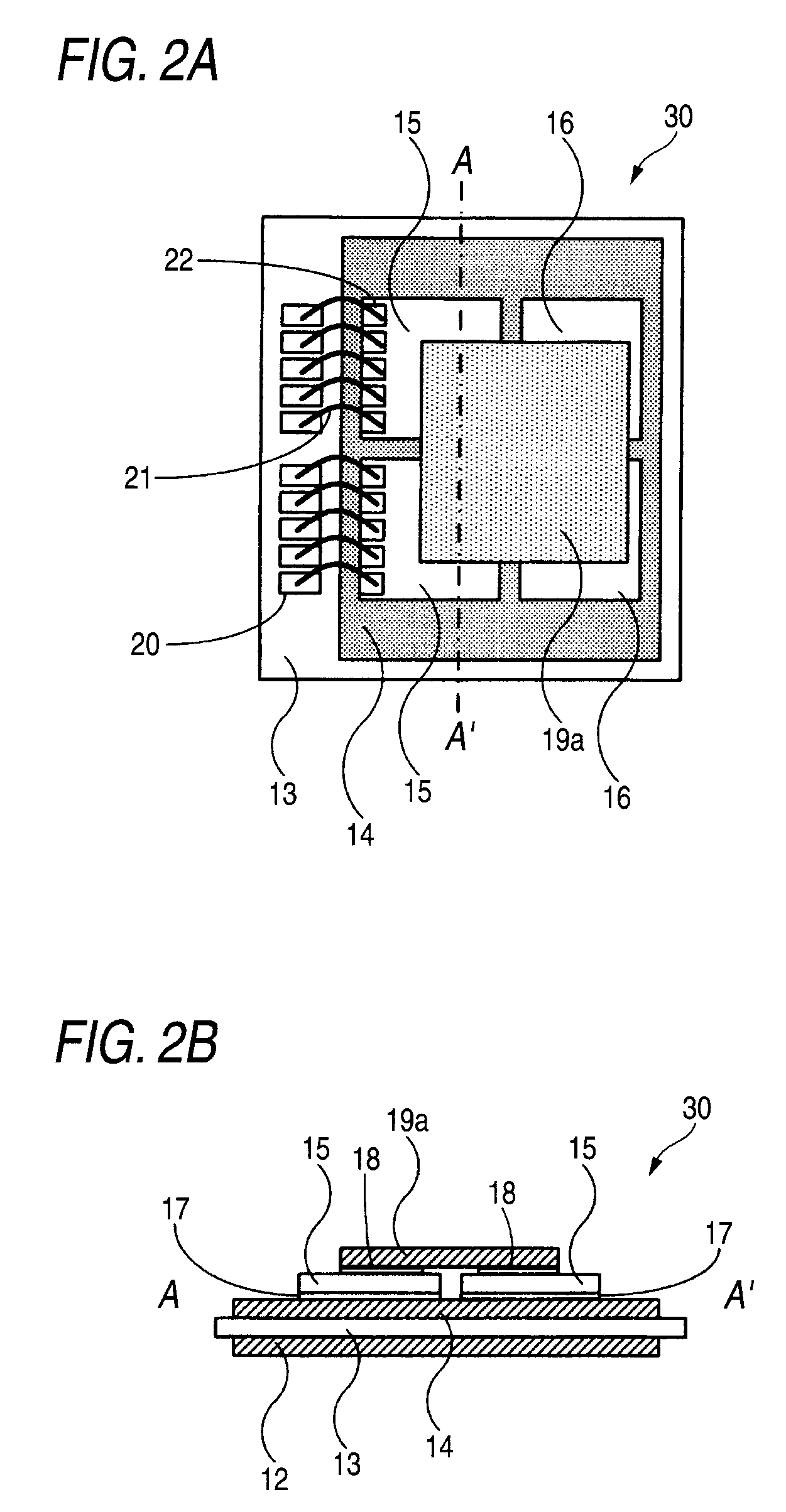
[0038]The semiconductor device 10 has a Cu foil 12 (not shown in FIG. 1A) soldered onto a Cu base 11, and an insulting substrate 13 joined onto the Cu foil 12 by the DCB method. A Cu foil 14a joined also by the...


PUM


Abstract

An electrical connection inside a semiconductor device is established by lead frames formed of plural conductor plates. The lead frames are disposed three-dimensionally so that the respective weld parts thereof are exposed toward a laser light source used in the laser welding. The laser welding is then performed by irradiating a laser beam. According to the above, welding can be performed readily in a reliable manner. The productivity of the semiconductor device and the manufacturing method of the semiconductor device can be thus enhanced. In addition, because the lead frames have the cooling effect, they have the capability of a heat spreader. It is thus possible to provide a semiconductor device and a manufacturing method of the semiconductor device with high productivity.

Description

CROSS-REFERENCE TO RELATED APPLICATION[0001]This reference claims priority from Japanese Application JP 2006-281694 filed on Oct. 16, 2006, the contents of which are incorporated herein by reference.BACKGROUND OF THE INVENTION[0002]The present invention relates to a semiconductor device and a manufacturing method of the semiconductor device, and more particularly, to a semiconductor device manufactured with the use of the laser welding technique and a manufacturing method of the semiconductor device.[0003]As a power converter, such as an industrial converter, a semiconductor device incorporating a semiconductor element, such as an IGBT (Insulated Gate Bipolar Transistor), has been used (for example, see JP-A-2005-116702). FIG. 16 is a schematic cross section of the major portion of a semiconductor device. In a semiconductor device 100, a Cu (copper) base 102 is joined to the bottom of an insulating substrate 101 via a solder 103, and a resin case 105 molded to enclose an IGBT elemen...

Claims


Application Information

Patent Timeline
IPC IPC(8): H01L23/495H01L21/60
CPCH01L23/3735H01L23/49811H01L24/29H01L24/33H01L24/40H01L24/41H01L24/45H01L24/48H01L24/49H01L24/73H01L24/84H01L25/072H01L25/162H01L25/18H01L25/50H01L2224/45124H01L2224/48091H01L2224/48175H01L2224/48227H01L2224/48247H01L2224/49111H01L2224/49175H01L2224/73219H01L2224/73221H01L2224/83224H01L2224/85205H01L2924/01005H01L2924/01013H01L2924/01014H01L2924/01015H01L2924/01028H01L2924/01029H01L2924/0105H01L2924/0106H01L2924/01074H01L2924/01078H01L2924/01079H01L2924/01082H01L2924/014H01L2924/13055H01L2924/30105H01L2924/30107H01L2924/01006H01L2924/01023H01L2924/01033H01L2924/01068H01L2224/73265H01L2924/12041H01L2224/40137H01L2924/1305H01L2924/00014H01L2924/00H01L2924/181H01L2224/37011H01L2224/05553H01L2924/19107H01L2224/37144H01L2224/84801H01L2224/37147H01L2224/83801H01L2224/37111H01L2224/3754H01L2224/371H01L24/37H01L2224/2612H01L2224/0603H01L2924/00012
Inventor YOKOMAE, TOSHIYUKIUEYANAGI, KATSUMICHIMOCHIZUKI, EIJIIKEDA, YOSHINARI
Owner FUJI ELECTRIC CO LTD
Why Eureka
Try Eureka