Cml circuit

a circuit and circuit technology, applied in the field of circuits, can solve the problems of power consumption rise when generating high frequency differential signals, disturbance of the fast operation of the ecl circuit, and inability to input signals with large amplitudes, etc., to achieve the effect of shortening the time of rising or falling and fast operation

Inactive Publication Date: 2008-06-26
NEC ELECTRONICS CORP
View PDF1 Cites 7 Cited by
  • Summary
  • Abstract
  • Description
  • Claims
  • Application Information

AI Technical Summary

Benefits of technology

[0016]The CML circuit of the present invention forms a differential pair with the first and second MOS transistors, thereby inputting a differential signal generated by an internal signal generation circuit and having an amplitude to be ranged approximately from a ground potential to a power supply potential without changing the signal amplitude. In addition, the employment of the third and fourth MOS transistors makes it possible to shorten...

Problems solved by technology

This is why the CML circuit 100 causes a problem that the power consumption rises when generating high frequency differential signals.
However, the ECL circuit 200 has a problem that it is impossible to input a signal having an amplitude large enough to enable switching between PMOS transistors M21 and M22 to the base of e...

Method used


Image

  • Cml circuit
  • Cml circuit
  • Cml circuit

Examples


first embodiment

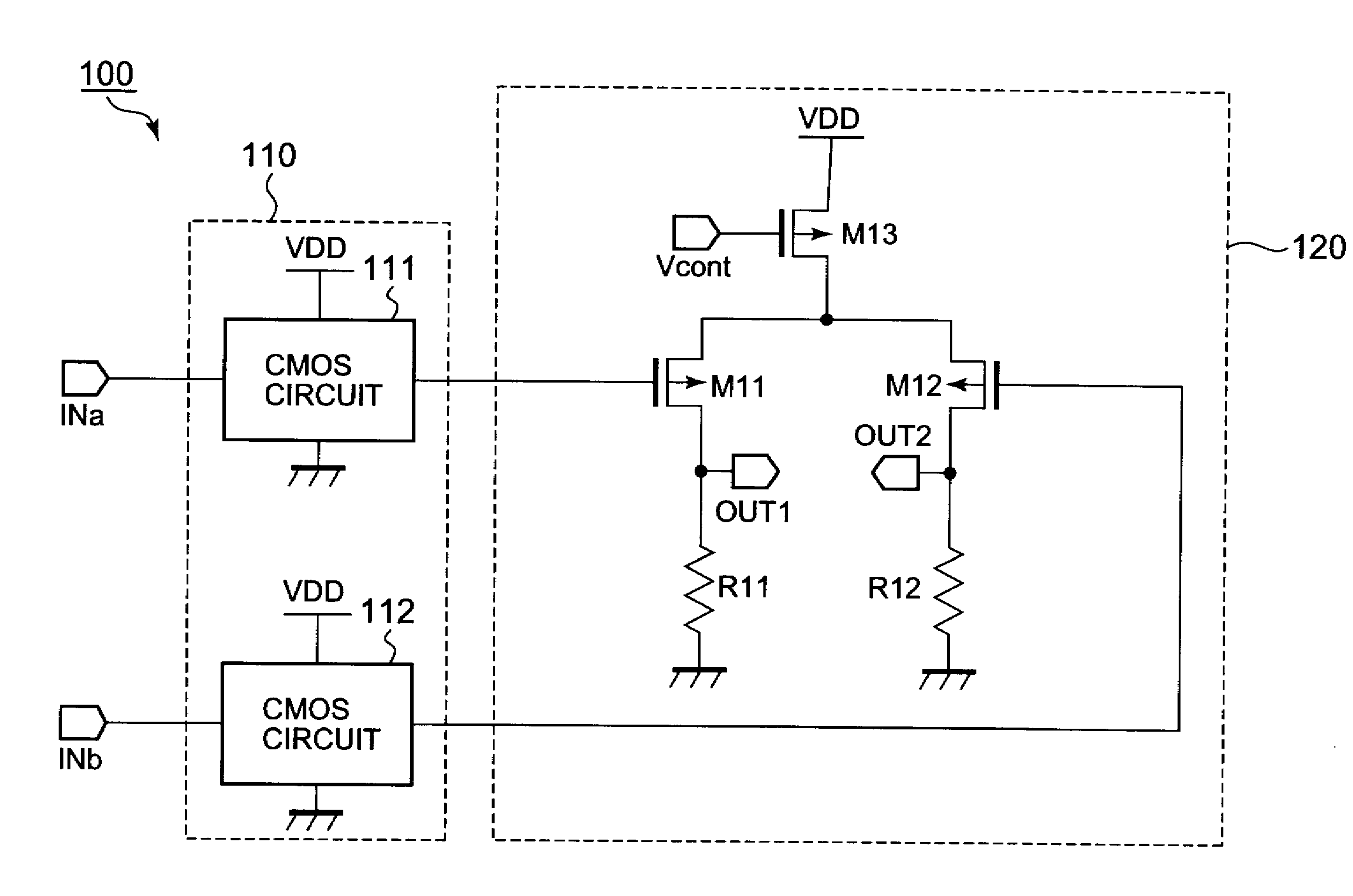
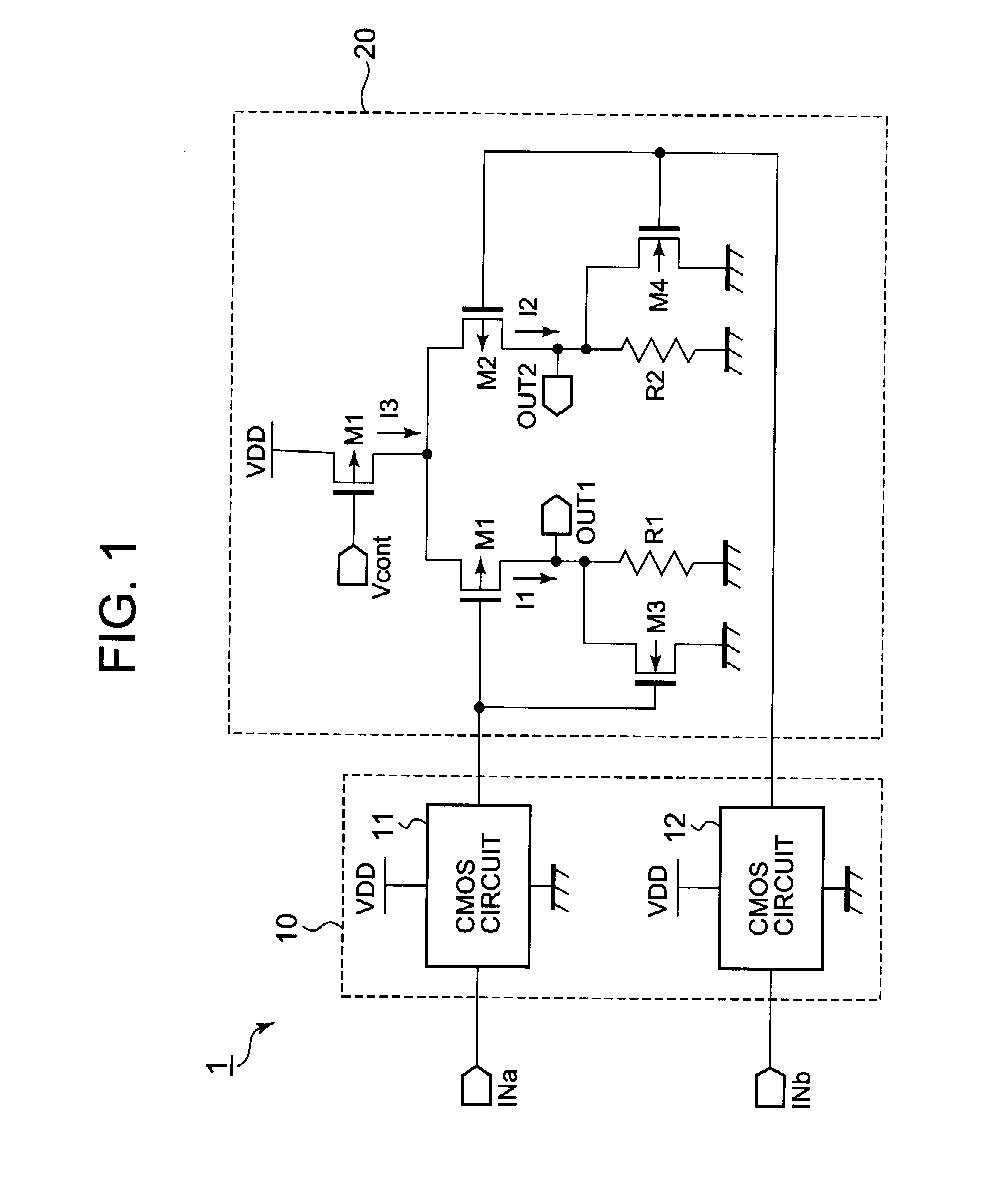
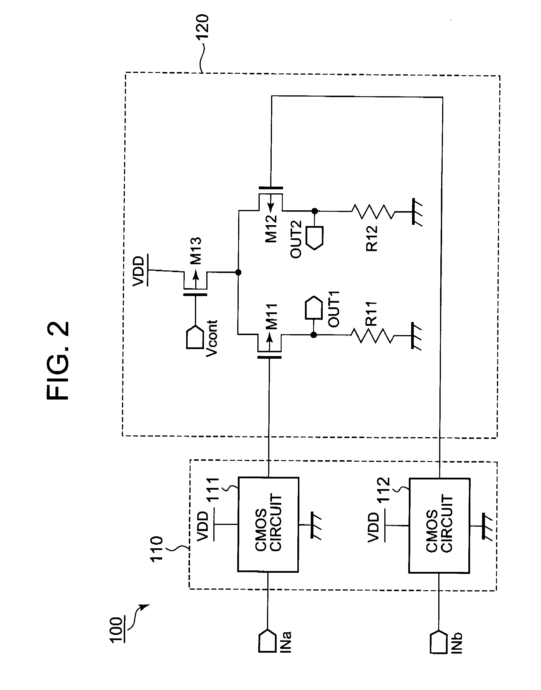
[0021]Hereunder, there will be described an embodiment of the present invention with reference to the accompanying drawings. FIG. 1 shows a circuit diagram of a CML circuit 1 in this first embodiment. The CML circuit 1 is driven according to a ground potential GND supplied from a first power supply terminal (e.g., a ground terminal) and a power supply potential VDD supplied from a second power supply terminal (e.g., a power supply terminal).

[0022]As shown in FIG. 1, the CML circuit 1 includes an internal signal generation circuit 10 and an amplification circuit 20. The internal signal generation circuit 10 includes CMOS circuits 11 and 12. Each of the CMOS circuits 11 and 12 is driven according to the power supply potential VDD and the ground potential GND and outputs a signal having an amplitude to be ranged approximately from a ground potential to a power supply potential according to a signal inputted from corresponding one of the input terminals INa and INb. The output signal of...


PUM


Abstract

Disclosed herein is a CML circuit that can solve a conventional problem that it has been impossible to input a large amplitude signal to a differential pair. The CML circuit of the present invention includes an internal signal generation circuit for generating an input differential signal having an amplitude to be ranged approximately from a ground potential to a power supply potential, a first MOS transistor having a gate for inputting a differential signal having one of the two amplitudes, a second MOS transistor having a gate for inputting a differential signal having the other of the two amplitudes and having a common source shared with the first MOS transistor, a first resistance element connected between the drain of the first MOS transistor and a first power supply terminal, a second resistance element connected between the drain of the second MOS transistor and the first power supply terminal, a third MOS transistor connected to the first resistance element in parallel, and a fourth MOS transistor connected to the second resistance element in parallel.

Description

BACKGROUND OF THE INVENTION[0001]1. Field of the Invention[0002]The present invention relates to a CML circuit, more particularly to a CML circuit corresponding to an input signal having an amplitude to be ranged approximately from a ground potential to a power supply potential.[0003]2. Description of Related Art[0004]In recent years, data communication speed in or between semiconductor devices has remarkably been improved. In order to cope with such fast data communications, amplitudes of signals to be sent and received are reduced to improve the signal frequencies. And now differential signals with high noise resistance are used for such fast data communications.[0005]An ECL (Emitter Coupled Logic) circuit and a CML (Current Mode Logic) circuit have been proposed to handle those differential signals having a small amplitude respectively. FIG. 2 shows an example of a general CML circuit 100 (conventional example 1). As shown in FIG. 2, the CML circuit 100 includes PMOS transistors ...

Claims


Application Information

Patent Timeline
IPC IPC(8): H03K19/094H03K19/20
CPCH03K19/018528H03K19/01721
Inventor TANAKA, MAKOTO
Owner NEC ELECTRONICS CORP
Why Eureka
Try Eureka