Power converting apparatus with dynamic driving adjustment
a technology of dynamic driving adjustment and power conversion apparatus, which is applied in the direction of electric variable regulation, process and machine control, instruments, etc., can solve the problems of not improving the emi issue, the power conversion efficiency is adversely affected, and the first gate resistor rgb>1/b> and the second gate resistor rgb>2/b> cannot be dynamically changed during the conversion period, so as to improve the whole power conversion efficiency, improve the emi
- Summary
- Abstract
- Description
- Claims
- Application Information
AI Technical Summary
Benefits of technology
Problems solved by technology
Method used
Image
Examples
second embodiment
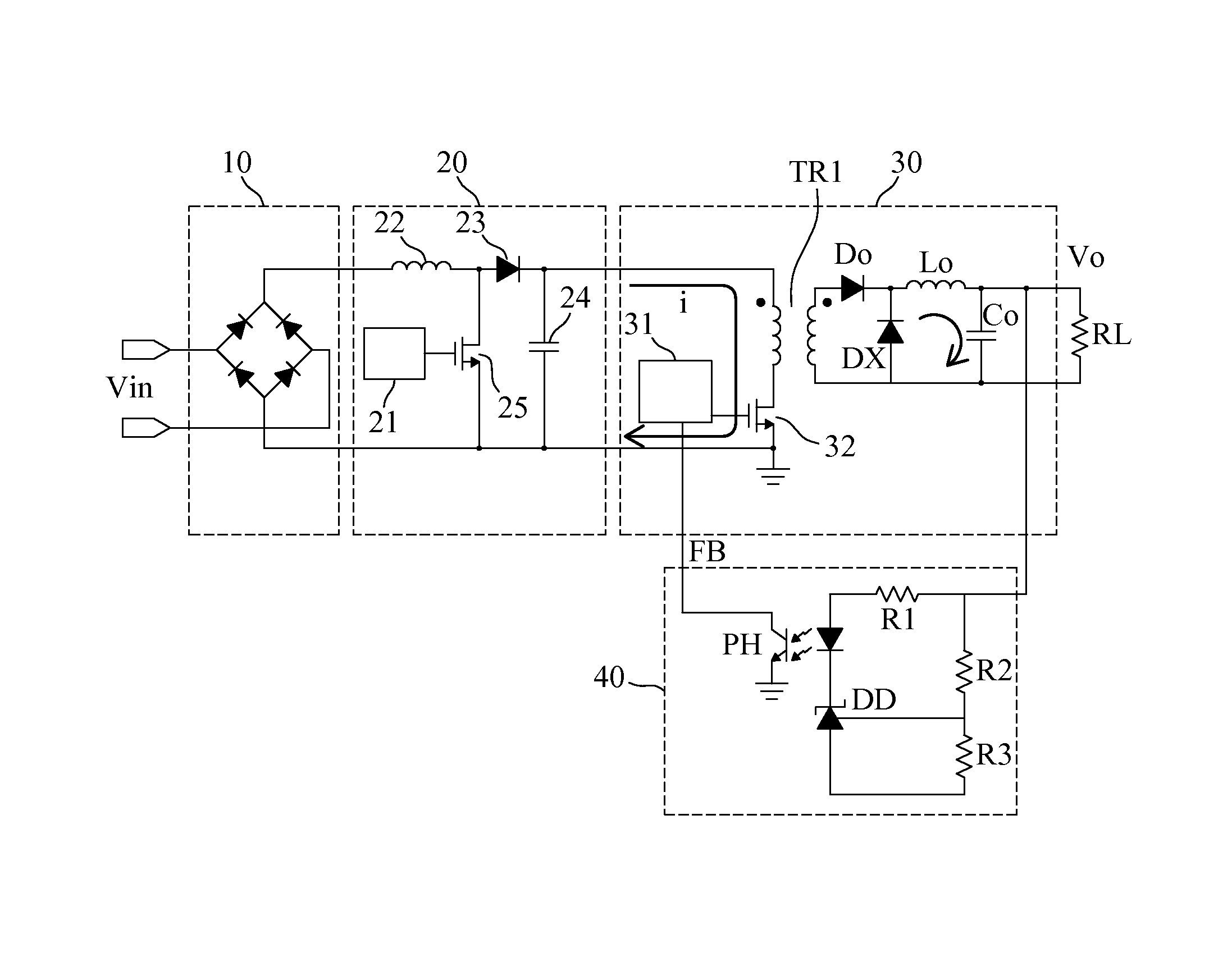
[0065]As shown in FIG. 7, except the structure of the PWM driving controller 31, other components of the power conversion unit 30 are similar to the second embodiment, and thus the description about the similar components are omitted. The PWM driving controller 31 is a full bridge structure and comprises a transformer TR2, four switch transistors Q1, Q2, Q3 and Q4, an auxiliary diode DX, an output inductor Lo, an output diode o and an output capacitor Co. The transformer TR2 comprises the first side coil and the second side coil with a center tap end. One end of the second side coil is connected to a positive end of the output diode Do, another end of the second side coil is connected to a positive end of the auxiliary coil, a negative end of the output diode Do is connected to a negative end of the auxiliary coil and one end of the output inductor Lo, another end of the output inductor Lo is connected to one end of the output capacitor Co, and another end of the output capacitor Co...
fifth embodiment
[0067]The switch transistors Q1, Q2, Q3 and Q4 shown in FIG. 7 are implemented by NPN bipolar transistors, and each of the switch transistors Q1, Q2, Q3 and Q4 shown in FIG. 8 is NMOS. Further, the present invention in FIG. 9 uses two PMOS transistors and two NMOS transistors, which operate as the above transistors, and the related electrical operation is thus omitted.
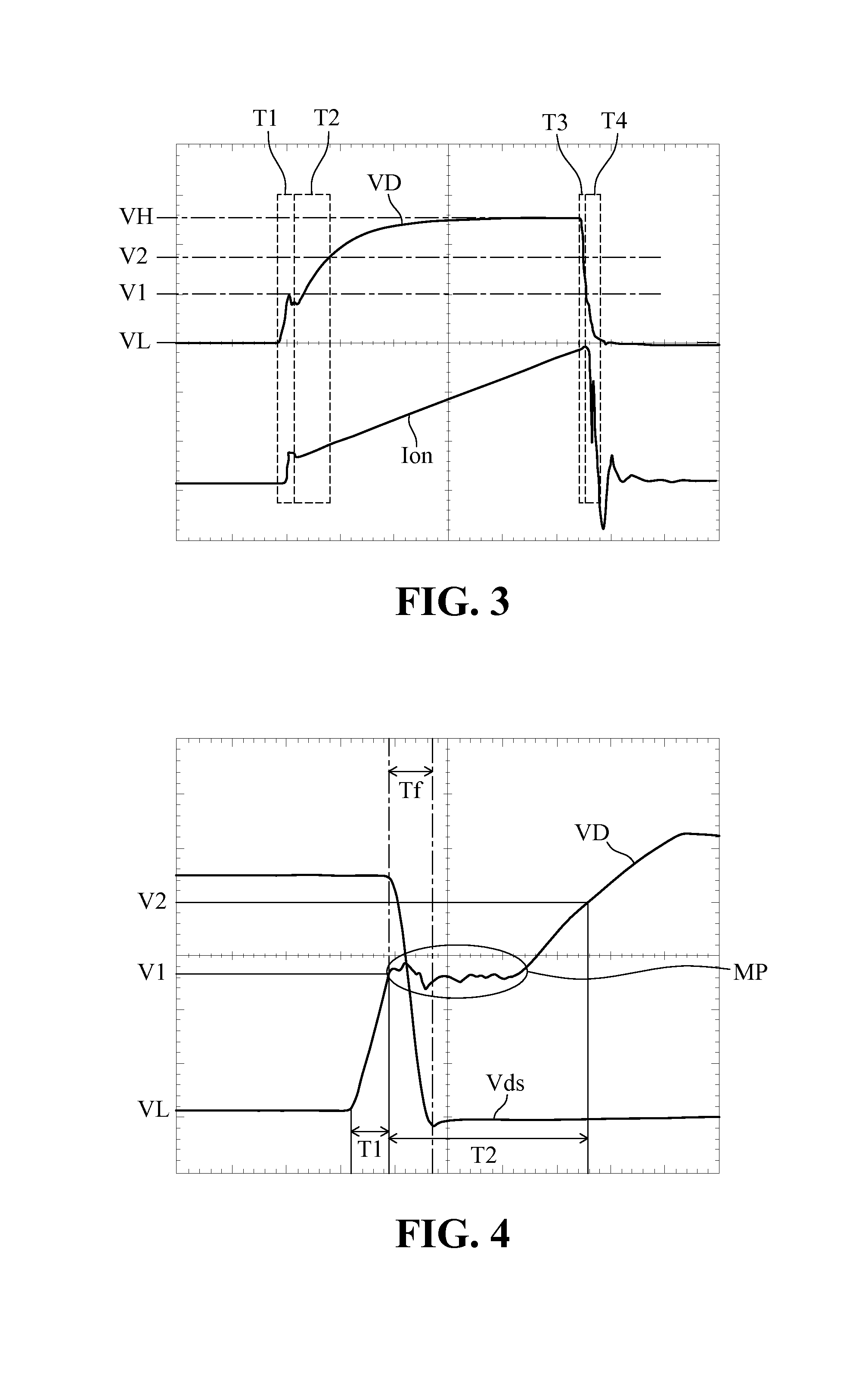
[0068]FIG. 10 typically shows the operation waveform for the PWM driving signal VD′ of the PMOS switch transistor Q1 or Q3 of the fifth embodiment in FIG. 9. The waveform also indicates the first rising period T1′, the second rising period T2′, the first falling period T3′ and the second falling period T4′ for the PMOS Q1 or Q3. It should be noted that the waveform of the switch transistor of PMOS is basically opposite in phase to the waveform of NOMS, and the operation of rising and falling is reversed so as to properly turn on and off the four switch transistors.
[0069]As shown in FIG. 11, the PWM driving controller 3...
PUM
 Abstract
Description
Claims
Application Information


