Methods for depth profiling in semiconductors using modulated optical reflectance technology

a modulated optical reflectance and semiconductor technology, applied in the field of depth profiling in semiconductors using modulated optical reflectance technology, can solve the problems of reducing the total mor signal at certain experimental conditions, and affecting the accuracy of depth profiling

Active Publication Date: 2008-06-26
KLA TENCOR TECH CORP
View PDF18 Cites 18 Cited by
  • Summary
  • Abstract
  • Description
  • Claims
  • Application Information

AI Technical Summary

Problems solved by technology

As a result, subsurface features such as damage produced by ion implantation, defects and non-uniformity of carrier concentration, alter the passage of the thermal and plasma waves and have a direct effect on the optical reflective patterns at the surface of the sample.
The difference in sign results in destructive interference between the thermal and plasma waves and decreases the total MOR signal at certain experimental conditions.
However, such is not the case in real semiconductor manufacturing and profile information should be extracted from the sample for the accurate analysis of its characteristics.
All these techniques are expensive, slow and destructive, i.e., require a special blank monitor wafer for analysis.
In addition, production SIMS tools can not currently provide reliable concentration profile information below 100 A. Spreading resistance measurements are faster than SIMS and RBS but not accurate enough in its depth profiling capability.
Also, RS technology requires good electrical contacts on both sides of semiconductor wafer which is not possible in most practical situations.
The solution to the inverse problem often involves sophisticated mathematical procedures, fitting algorithms, etc. and, therefore, is usually much more difficult to solve than the forward problem.
Finding a solution to the inverse problem, especially for depth profiles in semiconductors, represents the biggest challenge in metrology.
In addition, the solution to the inverse problem was not proposed in this study.
This fundamental limitation of plasma waves makes it impossible to use frequency domain measurements for electronic parameter depth profiling in semiconductors.
Therefore, box-like profiles can not be used for the accurate reconstruction of depth profiles.
A very few attempts to solve the inverse part of this depth profiling problem have failed to provide an accurate, reliable and sensitive enough technique that is required for applications in modern semiconductor manufacturing.

Method used


Image

  • Methods for depth profiling in semiconductors using modulated optical reflectance technology
  • Methods for depth profiling in semiconductors using modulated optical reflectance technology
  • Methods for depth profiling in semiconductors using modulated optical reflectance technology

Examples


Embodiment Construction

[0036]The present invention provides two different methods for depth profiling of parameters of interest in semiconductor materials using the MOR methodology. The first method is based on a simple reconstruction of the approximate depth profiles using experimental parameter values measured at certain depths below the surface of a sample. The second technique is a full forward and inverse problem method that utilizes MOR signals obtained by varying the experimental parameters such as different lateral beam offset distances (pump and probe beam separations), different modulation frequencies and / or different pump and probe beam wavelengths.

Apparatus Description

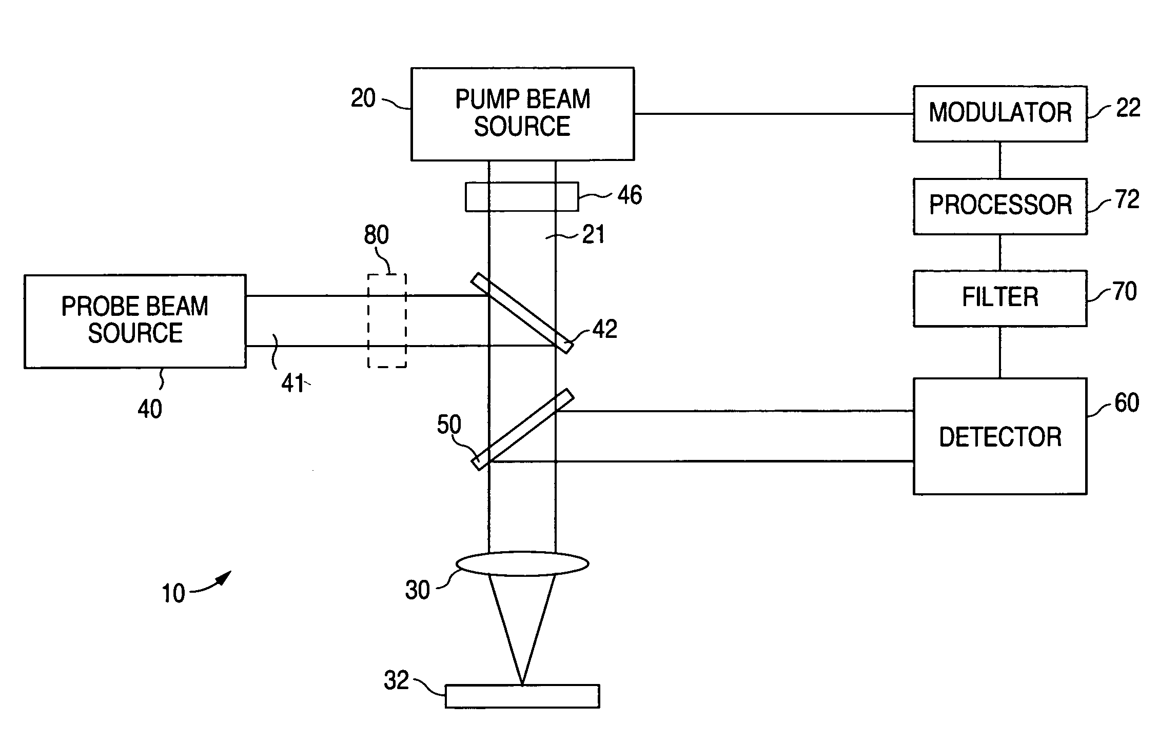
[0037]A schematic diagram of the MOR system capable of obtaining the measurements necessary to perform the methods of the subject invention is illustrated in FIG. 3.

[0038]System 10 includes a light source 20 for generating a pump beam of radiation 21. Pump beam source may be an intensity modulated laser or incoherent light source...


PUM

PropertyMeasurementUnit
wavelengthaaaaaaaaaa
modulation frequencyaaaaaaaaaa
spot sizeaaaaaaaaaa

Abstract

Methods of obtaining dopant and damage depth profile information are disclosed using modulated optical reflectivity (MOR) measurements. In one aspect, the depth profile is constructed using information obtained from various measurements such as the junction depth, junction abruptness and dopant concentration. In another aspect, a full theoretical model is developed. Actual measurements are fed to the model. Using an iterative approach, the actual measurements are compared to theoretical measurements calculated from the model to determine the actual depth profile.

Description

PRIORITY[0001]This application claims priority to U.S. Provisional Patent Application No. 60 / 876,247, filed Dec. 21, 2006, the disclosure of which is incorporated herein by reference.TECHNICAL FIELD[0002]The subject invention relates generally to optical methods for inspecting and analyzing semiconductor wafers and other samples. In particular, the subject invention relates to methods for obtaining depth profiles information about the thermal and electronic properties, damage and defects in semiconductor wafers.BACKGROUND OF THE INVENTION[0003]There is a great need in the semiconductor industry for metrology equipment that can provide high resolution, nondestructive evaluation of product wafers as they pass through various fabrication stages. In recent years, a number of products have been developed for the nondestructive evaluation of semiconductor samples. One such product has been successfully marketed by the assignee herein under the trademark Therma-Probe (TP). This device inco...

Claims


Application Information

Patent Timeline
Patent Type & Authority Applications(United States)
IPC IPC(8): G01N21/55
CPCG01N21/1717G01N2021/178G01N2021/1719
Inventor SALNIK, ALEXOPSAL, JONNICOLAIDES, LENA
Owner KLA TENCOR TECH CORP
Why Eureka
Try Eureka