Electrostatic discharge protection device and layout thereof

a protection device and electrostatic discharge technology, applied in semiconductor devices, semiconductor/solid-state device details, transistors, etc., can solve the problems of weakening the esd protection ability, unable to trigger the internal parasitic transistors unable to bypass the esd current in time to protect the core circuit, etc., to achieve the effect of enhancing the output driving ability of the core circui

Active Publication Date: 2008-06-26
AMAZING MICROELECTRONICS
View PDF9 Cites 25 Cited by
  • Summary
  • Abstract
  • Description
  • Claims
  • Application Information

AI Technical Summary

Benefits of technology

[0015]An ESD protection device provided by the present invention can be applied to an output buffer with ESD protection ability which receives an output signal from the core circuit to control the ESD protection device to output an external signal, so as to enhance the output driving ability of the core circuit.
[0016]An ESD protection layout provided by the present invention is an implementation of the above ESD protection device. In a limited layout area, a doped region is disposed in the substrate, and a bias conducting wire is used to electrically connect the doped region, thus the base coupling manner of the parasitic transistors in the ESD protection device is completed. Under a high voltage ESD, the parasitic transistors can be triggered simultaneously to bypass the ESD current in time, so as to avoid the non-uniform problem of bypassing the ESD current.

Problems solved by technology

As the NMOS transistor that has been broken down lowers the potential of the conducting wire coupled thereto, the ESD pulse will not trigger other NMOS transistors, thus causing a non-uniform problem of bypassing the ESD current and weakening the ESD protection ability.
However, the layout of embedding the P+ diffusion region 306 not only increases the layout area, but also results in an over low substrate resistance of the NMOS transistor in a deep-submicron complementary metal-oxide-semiconductor (CMOS) transistor process, thus making it difficult to trigger the internal parasitic transistors and bypass the ESD current in time to protect the core circuit.
However, the high bias applied on the gate of the NMOS transistor MN1 / PMOS transistor MP1 may generate a larger channel current, and a higher electric field may cause the breakdown of a thin gate-oxide layer, thus weakening the ESD protection ability.
However, though the non-uniform problem of bypassing the ESD current can be solved by the above conventional art, the complexity of the layout is increased.

Method used


Image

  • Electrostatic discharge protection device and layout thereof
  • Electrostatic discharge protection device and layout thereof
  • Electrostatic discharge protection device and layout thereof

Examples


Embodiment Construction

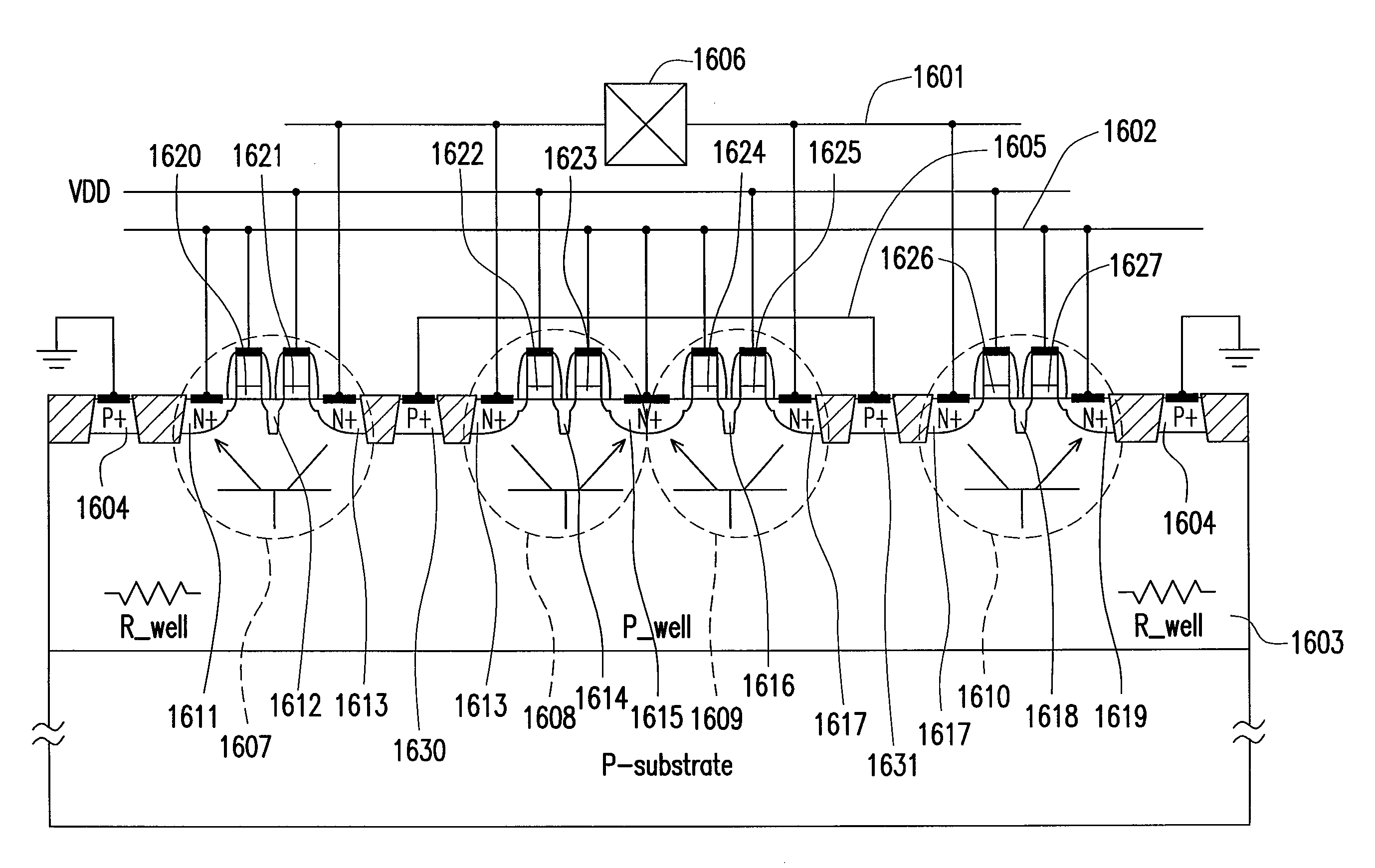
[0048]FIG. 7 is an ESD protection device according to a preferred embodiment of the present invention. Referring to FIG. 7, an ESD protection device 703 is coupled between a pad 701 and a second conductive path (for example, a ground voltage trace) 702. The pad 701 is coupled to a core circuit 706 via a first conductive path, and the pad 701 can be an input pad or an output pad. The ESD protection device 703 mainly includes ESD protection units 707-710 and a bias conducting wire 705. This embodiment adopts, for example, a multi-finger type layout manner to implement the ESD protection device 703, so as to reduce the occupied silicon area. Herein, only four ESD protection units 707-710 are taken as an example for illustration, and those of ordinary skill in the art can determine the number of the ESD protection unit as required.

[0049]Each of the ESD protection units 707-710 in this embodiment has an NMOS transistor (i.e., M1-M4 in FIG. 7). As the NMOS transistors M1-M4 are disposed i...


PUM


Abstract

An electrostatic discharge (ESD) protection device and a layout thereof are provided. A bias conducting wire is mainly used to couple each base of a plurality of parasitic transistors inside ESD elements together, in order to simultaneously trigger all the parasitic transistors to bypass the ESD current, avoid the elements of a core circuit being damaged, and solve the non-uniform problem of bypassing the ESD current when ESD occurs. Furthermore, in the ESD protection layout, it only needs to add another doped region on a substrate neighboring to, but not contacting, doped regions of the ESD protection elements and use contacts to connect the added doped region, so as to couple each base of the parasitic transistors together without requiring for additional layout area.

Description

BACKGROUND OF THE INVENTION[0001]1. Field of the Invention[0002]The present invention relates to an ESD protection device and a layout thereof. More particularly, the present invention relates to an ESD protection device with equal-substrate-potential technology and a layout thereof.[0003]2. Description of Related Art[0004]Electronic products are often impacted by ESD in practical use. Generally speaking, an ESD voltage is much higher than a common supply voltage, and discharge models can be classified into human-body model (HBM), machine model (MM), and charge-device model (CDM) based on different voltage levels generated by ESD. When ESD occurs, the ESD current is likely to burn the elements, such that some ESD protection measures must be taken in the circuit to effectively isolate the ESD current, so as to prevent the elements from being damaged.[0005]Commonly, a design of ESD protection device is disposed between a core circuit and a pad to protect internal circuits. There are s...

Claims


Application Information

Patent Timeline
Patent Type & Authority Applications(United States)
IPC IPC(8): H02H9/00
CPCH01L27/027H01L2924/0002H01L2924/00
Inventor KER, MING-DOUCHEN, JIA-HUEIJIANG, RYAN HSIN-CHIN
Owner AMAZING MICROELECTRONICS
Why Eureka
Try Eureka