Manufacturing method of display device

Active Publication Date: 2008-06-26
PANASONIC LIQUID CRYSTAL DISPLAY CO LTD +1
View PDF9 Cites 30 Cited by
  • Summary
  • Abstract
  • Description
  • Claims
  • Application Information

AI Technical Summary

Benefits of technology

[0047]The representative effect of the invention is as follows.
[0048]When the transparent substrate is bonded with the display panel via the adhesive,

Problems solved by technology

Accordingly, a coating process becomes complex.
Further, there occurs a step with the high viscosity adhesive unles

Method used


Image

  • Manufacturing method of display device
  • Manufacturing method of display device
  • Manufacturing method of display device

Examples


embodiment 1

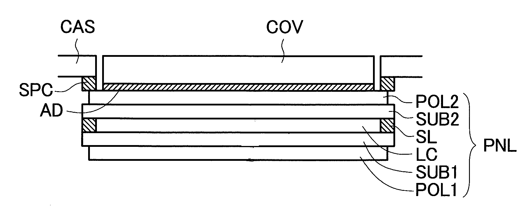
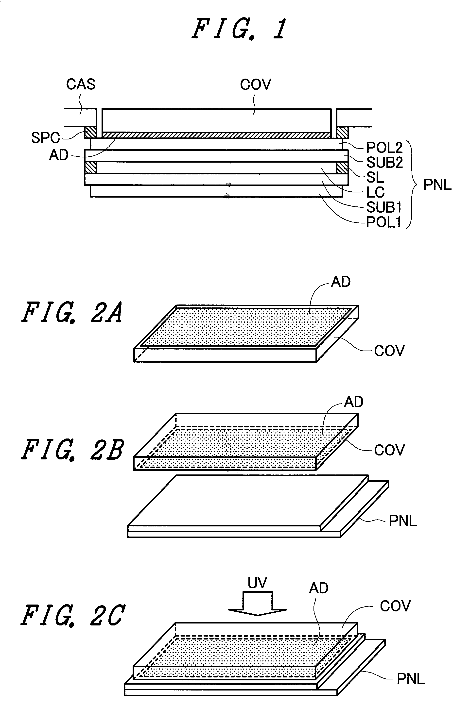
[0062]FIG. 1 is across-sectional view for explaining one example of a display device according to an embodiment 1 of the invention. In the embodiment 1, a liquid crystal display is used for a display panel PNL. In FIG. 1, the display panel PNL such as a liquid crystal display panel is incorporated into a casing CAS for a portable telephone or the like. The display panel PNL has a substrate SUB1 that is a translucent insulating substrate made of glass or the like, a substrate SUB2 that is a translucent insulating substrate made of glass or the like, a sealing material SL for bonding the substrate SUB1 and the substrate SUB2, a liquid crystal LC sealed into the inside surrounded by the substrate SUB1, the substrate SUB2 and the sealing material SL, a polarizer POLL disposed on the side of the substrate SUB1 opposite to the liquid crystal LC, and a polarizer POL2 disposed on the side of the substrate SUB2 opposite to the liquid crystal LC. Also, a thin film transistor and a pixel elect...

embodiment 2

[0078]FIG. 7 is a side view for explaining one example of a manufacturing method of a display device according to an embodiment 2 of the invention. When the display panel PNL and the transparent substrate COV are bonded, they are bonded while the display panel PNL is bent to be convex on the side of bonding face, as shown in FIG. 7. Thereby, the possibility that large bubbles are entrained can be reduced. In this case, it is preferable that the total of the thickness t1 of the substrate SUB1 and the thickness t2 of the substrate SUB2 is 0.8 mm or less, more preferably 0.6 mm or less. The lower limit is not particularly limited, but the total is desirably 0.1 mm or more.

[0079]Though the display panel PNL is bent in FIG. 7, the transparent substrate COV or both the display panel PNL and the transparent substrate COV may be bent so as to be convex on the side of bonding face during bonding.

embodiment 3

[0080]FIG. 8 is a cross-sectional view for explaining one example of a display device according to an embodiment 3 of the invention. A different point from the embodiment 1 of FIG. 1 is that the adhesive AD extends up to the end part of the polarizer POL2. The adhesive AD can be spread outside the end part of the transparent substrate COV, when bonded, by adjusting the viscosity of the adhesive AD, the coating pattern, or the coating amount, for example. Or the adhesive AD may be coated on the side of the display panel PNL.


PUM

PropertyMeasurementUnit
Temperatureaaaaaaaaaa
Lengthaaaaaaaaaa

Abstract

To prevent bubbles from remaining when a transparent substrate is bonded via an adhesive with a display panel. A manufacturing method of a display device in which a transparent substrate is bonded with a display panel via an adhesive, including a coating step of coating the adhesive onto the display panel or the transparent substrate in a predetermined pattern, a bonding step of bonding the display panel and the transparent substrate via the adhesive after the coating step, and a curing step of curing the adhesive after the bonding step, characterized in that the adhesive has a viscosity of 2000 to 5000 mPa·s at the coating step, the display panel and the transparent substrate are bonded via the adhesive in a reduced pressure atmosphere lower than the atmospheric pressure in a state where the adhesive coated at the coating step is spread and the size of bubble is 1 mm or less at maximum at the bonding step, and the adhesive is cured by applying ultraviolet ray at the curing step.

Description

[0001]The present application claims priority from Japanese application JP2006-346932 filed on Dec. 25, 2006, the content of which is hereby incorporated by reference into this application.BACKGROUND OF THE INVENTION[0002]1. Field of the Invention[0003]The present invention relates to a manufacturing method of a display device, and more particularly to a manufacturing method of a display device in which a transparent substrate (protection cover) is bonded with a display panel via an adhesive.[0004]2. Description of Related Art[0005]A display device such as a liquid crystal display is used in various sizes ranging from small portable telephones to large TV.[0006]FIG. 11 is a cross-sectional view for explaining the conventional liquid crystal display. In FIG. 11, a display panel PNL such as a liquid crystal display panel, for example, is incorporated into a casing CAS for the portable telephone.[0007]In the liquid crystal display panel, the display panel PNL has a substrate SUB1, a su...

Claims


Application Information

Patent Timeline
IPC IPC(8): G02F1/1333
CPCG02F1/133308G02F2202/28G02F2001/133311G02F1/133311G02F1/1339G02F1/13
Inventor KOBAYASHI, SETSUOMIWA, HIROAKIISHII, KATSUHIKOIWASAKI, SHUJI
Owner PANASONIC LIQUID CRYSTAL DISPLAY CO LTD
Why Eureka
Try Eureka