Light-emitting diode and method for manufacturing the same

a technology of light-emitting diodes and manufacturing methods, which is applied in the direction of semiconductor/solid-state device manufacturing, semiconductor devices, electrical devices, etc., can solve the problems of low yield, difficult process, and serious affecting the light-emitting efficiency of light-emitting diodes, so as to improve the current-spreading effect and improve the efficiency of light extraction. , the effect of enhancing the brightness of the light-emitting diodes

Active Publication Date: 2008-07-03
EPISTAR CORP
View PDF11 Cites 14 Cited by
  • Summary
  • Abstract
  • Description
  • Claims
  • Application Information

AI Technical Summary

Benefits of technology

[0006]One aspect of the present invention is to provide a light-emitting diode, which comprises a thicker window layer, so that the light-emitting diode has a better current-spreading effect, thereby increasing light extraction efficiency and enhancing brightness of the light-emitting diode.
[0007]Another aspect of the present invention is to provide a light-emitting diode, which is a P-side up structure, so that it is much easier to perform the roughening treatment of a surface of the light-emitting diode, thereby increasing light extraction efficiency and enhancing brightness.
[0008]Still another aspect of the present invention is to provide a method for manufacturing a light-emitting diode, in which a thicker window layer is grown on a growth substrate, so that the window layer can be a temporary supporting structure. Therefore, the removal of the growth substrate, the sequential processes of the illuminant epitaxial structure and some necessary processes of the permanent substrate can be completed before the wafer bonding process. Thus, the process window is greatly increased, and process yield can be effectively enhanced.
[0009]Further another aspect of the present invention is to provide a method for manufacturing a light-emitting diode, which can use an alloy having low fusion point as a medium for wafer bonding, so that the reliability of the wafer bonding process can be effectively enhanced.

Problems solved by technology

The growth substrate composed of N-type GaAs can absorb light, so that most of the photons produced by the active layer of the light-emitting diode while being emitted towards the growth substrate are absorbed by the growth substrate, thus seriously affecting the light emitting efficiency of the light-emitting diode device.
However, the U.S. Pat. No. 5,376,580 has disadvantages of difficult process and low yield caused by the need to consider the consistency of the lattice direction between the bonding wafers, since the bonding mediums are semiconductors.

Method used


Image

  • Light-emitting diode and method for manufacturing the same
  • Light-emitting diode and method for manufacturing the same
  • Light-emitting diode and method for manufacturing the same

Examples


Embodiment Construction

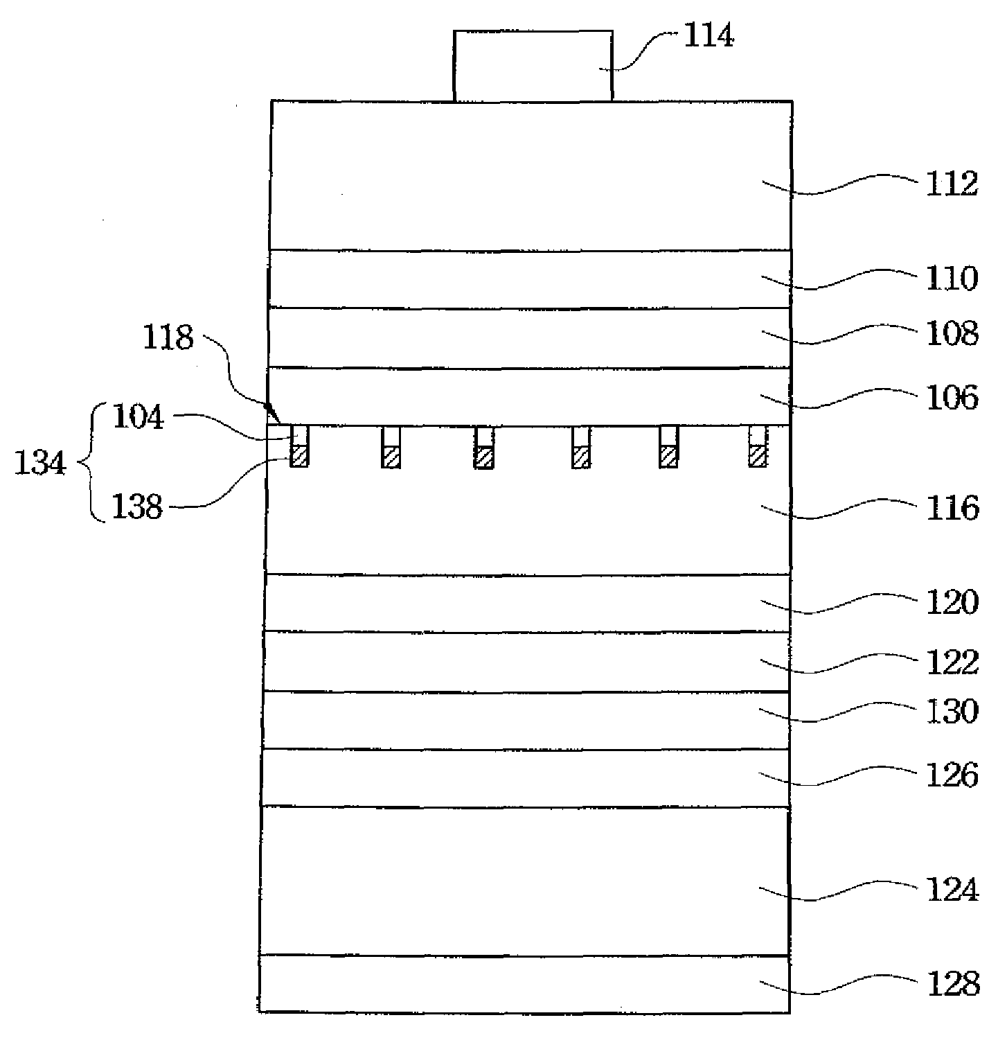
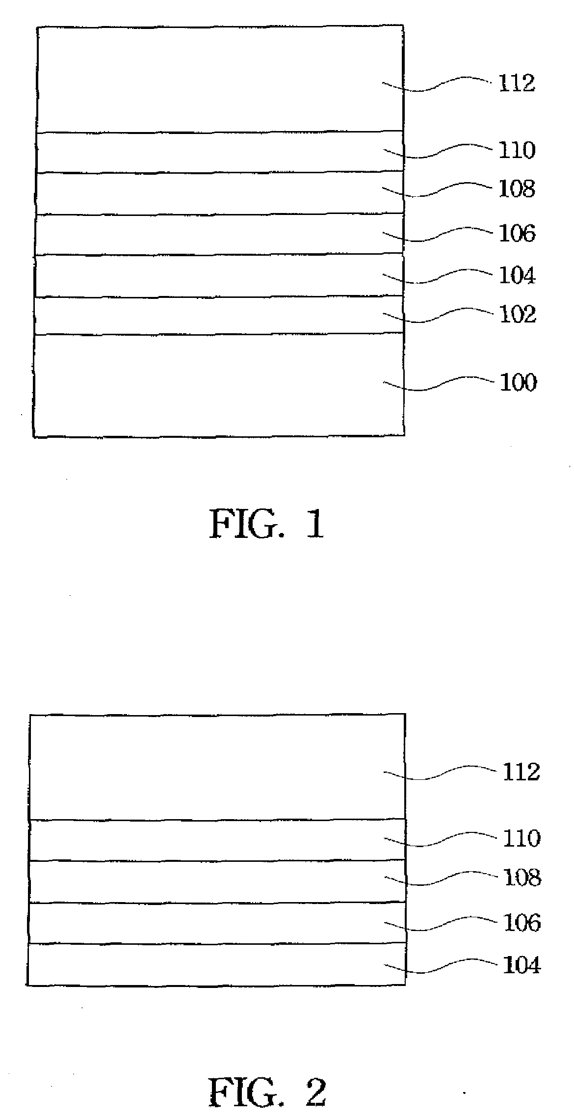
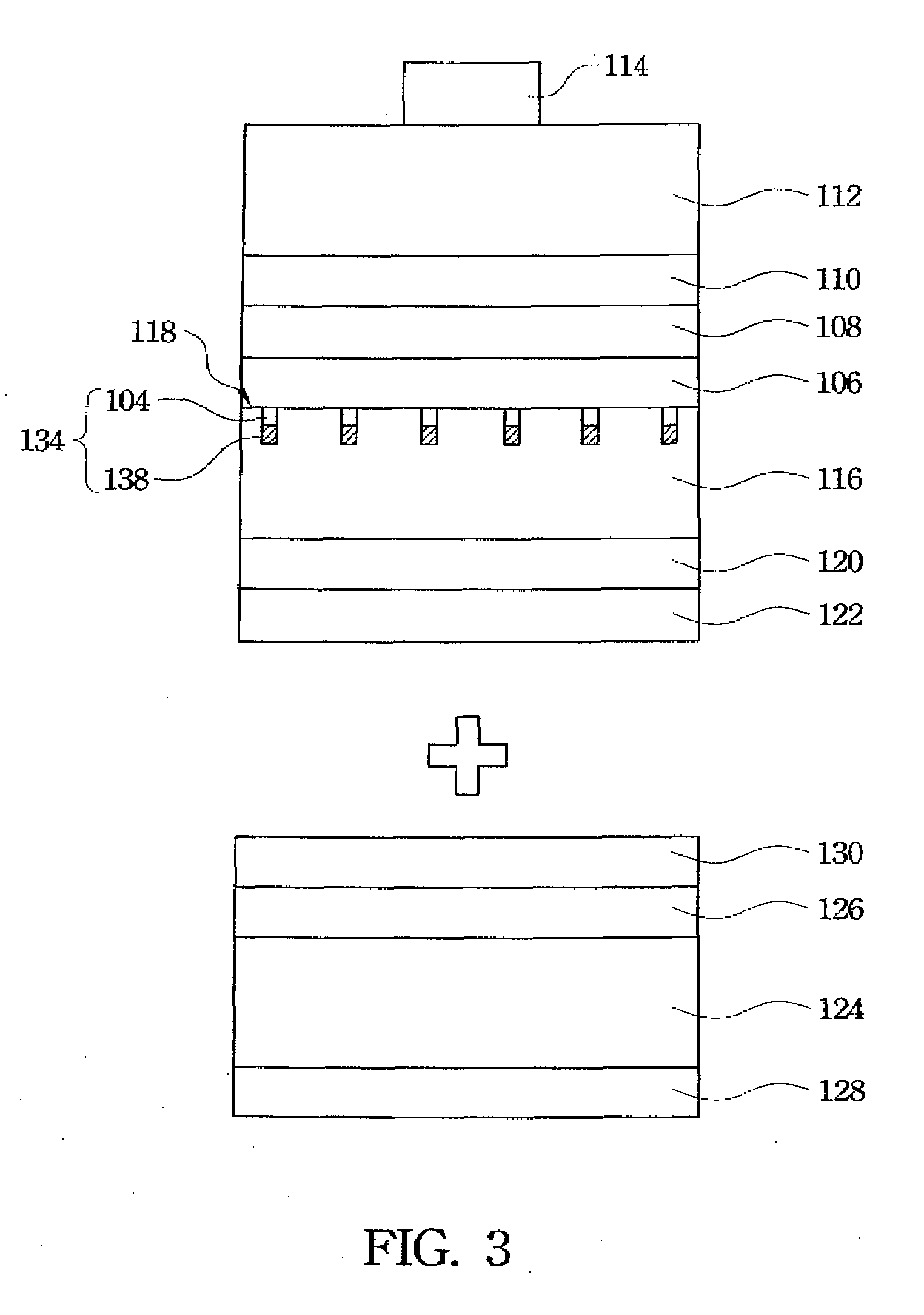
[0016]The present invention discloses a light-emitting diode and a method for manufacturing the same. The light-emitting diode has a thicker window layer, so that the current-spreading effect can be increased, light extraction efficiency can be enhanced, the roughening treatment of the light-emitting diode device is easier, thereby further enhancing light extraction efficiency and increasing brightness of the light-emitting diode device. Besides, the necessary processes can be completed before the wafer bonding step, so the bonding temperature is more flexible, and the process window is wider. Moreover, an alloy with a low fusion point may be used as a medium for wafer bonding, so that the reliability of the wafer bonding process can be improved. In order to make the illustration of the present invention more explicit, the following description is stated with reference to FIGS. 1 through 4.

[0017]FIGS. 1 through 4 are schematic flow diagrams showing the process for manufacturing a li...


PUM

PropertyMeasurementUnit
thicknessaaaaaaaaaa
thicknessaaaaaaaaaa
conductiveaaaaaaaaaa

Abstract

A light-emitting diode (LED) and a method for manufacturing the same are described. The light-emitting diode comprises: a conductive substrate including a first surface and a second surface opposite to the first surface; a metal bonding layer deposed on the first surface of the conductive substrate; a reflective metal layer deposed on the metal bonding layer; an N-type semiconductor layer deposed on the reflective metal layer; an active layer deposed on the N-type semiconductor layer; a P-type semiconductor layer deposed on the active layer; a window layer deposed on the P-type semiconductor layer, wherein a thickness of the window layer is substantially at least 50 μm, and the window layer is composed of a transparent conductive material; and a P-type electrode deposed on the window layer.

Description

RELATED APPLICATIONS[0001]The present application is based on, and claims priority from, Taiwan Application Serial Number 95150027, filed Dec. 29, 2006, the disclosure of which is hereby incorporated by reference herein in its entirety.FIELD OF THE INVENTION[0002]The present invention relates to a light-emitting diode (LED) and a method for manufacturing the same, and more particularly, to a high efficiency light-emitting diode and a method for manufacturing the same.BACKGROUND OF THE INVENTION[0003]In the fabrication of light-emitting diodes, III-V group compound semiconductors, such as GaN, AlGaN, InGaN and AlInGaN, are common. Usually, epitaxial structures of most of the light-emitting devices made of the III-V group compound semiconductors are grown on an electrically insulating sapphire substrate, which is different from other light-emitting devices utilizing conductive substrates. The sapphire substrate is an insulator, so an electrode cannot be directly formed on the sapphire...

Claims


Application Information

Patent Timeline
Patent Type & Authority Applications(United States)
IPC IPC(8): H01L33/00H01L21/329H01L33/06H01L33/14H01L33/30H01L33/42
CPCH01L33/0079H01L2933/0016H01L33/387H01L33/0093
Inventor SHEI, SHIH-CHANGHON, SCHANG-JINGWEI, SHIH-CHENSU, JUH-YUH
Owner EPISTAR CORP
Why Eureka
Try Eureka