Light emitting diode and method for manufacturing the same

Inactive Publication Date: 2005-01-06
EPISTAR CORP +1
View PDF7 Cites 9 Cited by
  • Summary
  • Abstract
  • Description
  • Claims
  • Application Information

AI Technical Summary

Benefits of technology

[0012] According to a preferred embodiment of the present invention, after the wafer bonding step is performed, the method further comprises etching a n-type semiconductor contact layer of the semiconductor structure to make the n-type semiconductor contact layer form a non-planar continuous structure or a discontinuous surface structure, so as to enhance current-spreading effect.
[0013] The loss of light intensity resulted from the absorbing of the substrate can be reduced greatly by removing the growth substrate

Problems solved by technology

However, the U.S. Pat. No. 5,376,580 has a disadvantage of low yield caused by the need of considering the consistency of the lattice direction between the bondin

Method used


Image

  • Light emitting diode and method for manufacturing the same
  • Light emitting diode and method for manufacturing the same
  • Light emitting diode and method for manufacturing the same

Examples


Embodiment Construction

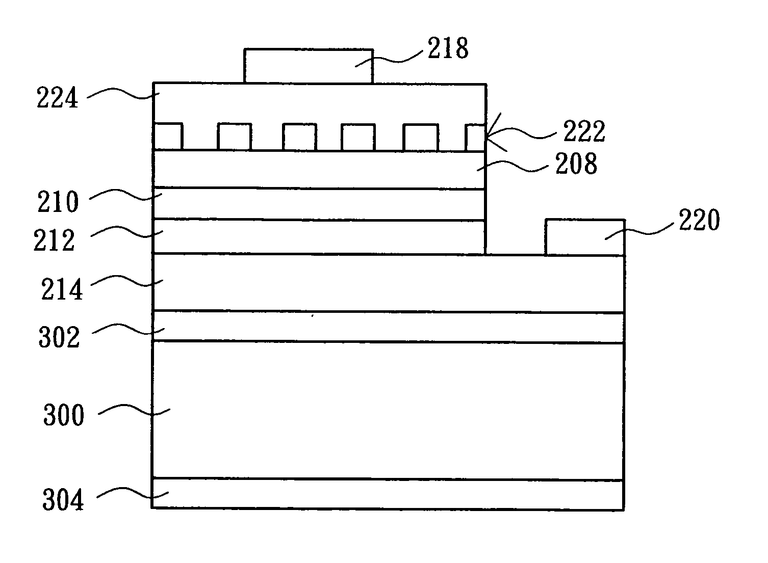
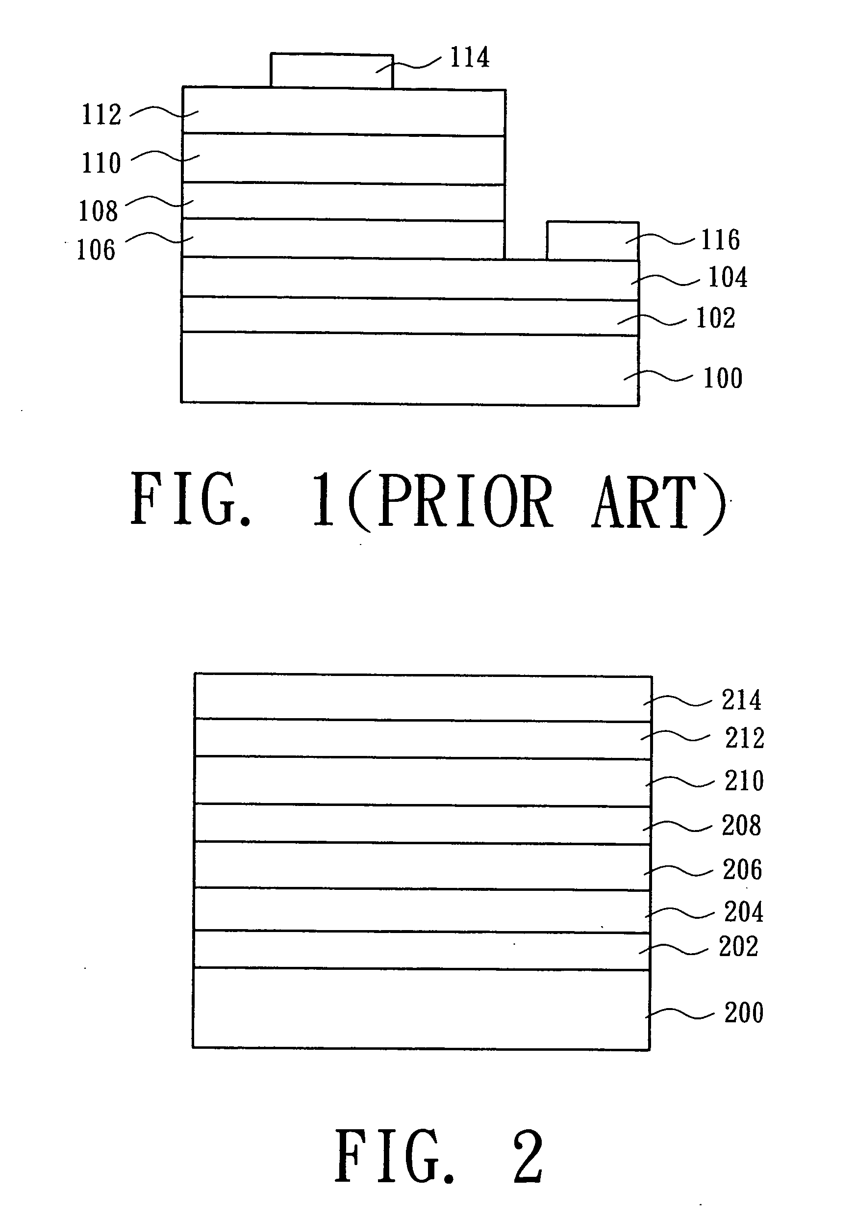
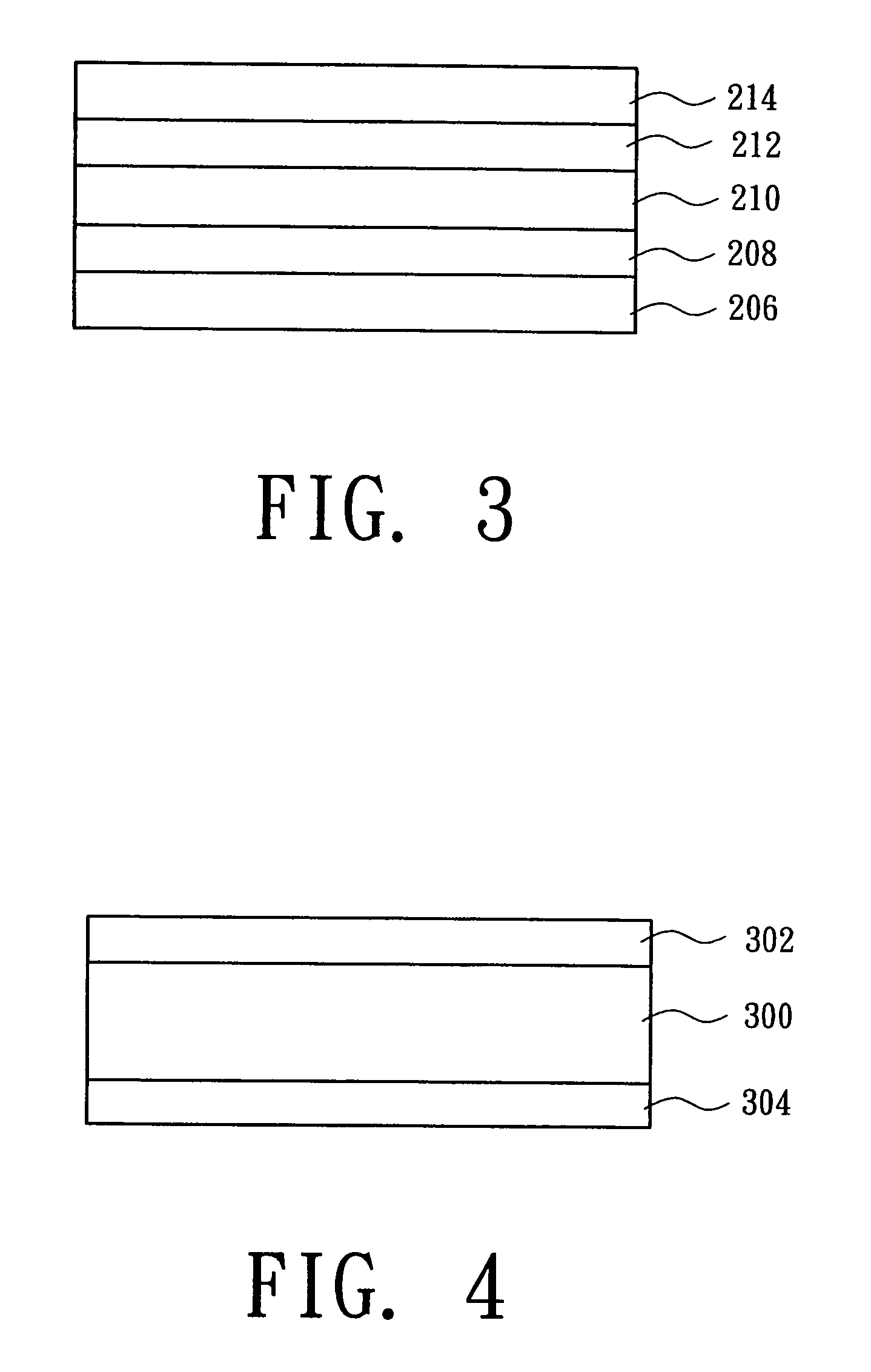
[0019] The present invention discloses a light emitting diode and a method for manufacturing the same. In order to make the illustration of the present invention more explicitly and completely, the following description and the drawings from FIG. 2 to FIG. 6 are stated.

[0020] Among semiconductor light emitting devices, AlGaInP is a very commonly-used material. Because AlGaInP is a kind of direct bandgap materials, appropriately adjusting the ratio of In / (Al+Ga) in the AlGaInP material can make the lattice constant of the AlGaInP material and the GaAs substrate matched. Adjusting the ratio of Al and Ga in the AlGaInP material can make light emitted between 550 nm (green light) and 680 nm (red light) in wavelength. It is very easy to adjust the AlGaInP material on the device epitaxy, so it is easy to obtain emitting light with desired wavelengths by a linear method, and AlGaInP is very suitable for use in manufacturing a light emitting device of visible light zone.

[0021] Besides, ad...


PUM


Abstract

A light emitting diode and a method for manufacturing the same are disclosed. The light emitting diode comprises: a transparent substrate; a reflective layer located on a surface of the transparent substrate; a solder layer located on the other surface of the transparent substrate; a semiconductor epitaxial structure located on the solder layer, wherein the semiconductor epitaxial structure comprises a n-type contact layer, and the n-type contact layer can be a structure having a continuous flat surface, a structure having a continuous reticulate or bar surface, or a cylinder or prism structure having a discontinuous surface; and a transparent conductive layer located on the n-type contact layer of the semiconductor epitaxial structure.

Description

FIELD OF THE INVENTION [0001] The present invention relates to a light emitting diode and a method for manufacturing the same, and more particularly, to a high-brightness light emitting diode manufactured by a wafer bonding technique. BACKGROUND OF THE INVENTION [0002] Referring to FIG. 1, FIG. 1 illustrates a cross-sectional view of a conventional light emitting diode. The light emitting diode comprises a substrate 100, a n-type semiconductor buffer layer 102, a n-type semiconductor contact layer 104, a n-type semiconductor cladding layer 106, an active layer 108, a p-type semiconductor cladding layer 110 and a p-type semiconductor contact layer 112 stacked in sequence. The light emitting diode further comprises a p-type contact pad 114 located on a portion of the p-type semiconductor contact layer 112, and a n-type contact pad 116 located on the exposed portion of the n-type semiconductor contact layer 104. [0003] The material of the substrate 100 of a conventional light emitting ...

Claims


Application Information

Patent Timeline
IPC IPC(8): H01L21/00H01L33/00H01L33/14H01L33/42H01L33/46
CPCH01L33/0079H01L33/02H01L33/46H01L33/42H01L33/14
Inventor CHEN, SHI-MING
Owner EPISTAR CORP
Why Eureka
Try Eureka