RF integrated circuit device

a technology of integrated circuits and circuits, applied in the direction of semiconductor devices, electrical devices, transistors, etc., can solve the problems of large parasitic capacitance generation, and achieve the effect of reducing layout area and parasitic capacitan

Inactive Publication Date: 2008-07-03
MEDIATEK INC
View PDF3 Cites 54 Cited by
  • Summary
  • Abstract
  • Description
  • Claims
  • Application Information

AI Technical Summary

Benefits of technology

[0005]A differential pair configuration of an integrated circuit for reducing layout area and parasitic capacitance is provided.

Problems solved by technology

In the conventional layout, the differential pair occupies too much layout area, easily generating large parasitic capacitance due to the metal connection.

Method used


Image

  • RF integrated circuit device
  • RF integrated circuit device
  • RF integrated circuit device

Examples


Embodiment Construction

[0016]The following description is of the best-contemplated mode of carrying out the invention. This description is made for the purpose of illustrating the general principles of the invention and should not be taken in a limiting sense. The scope of the invention is best determined by reference to the appended claims.

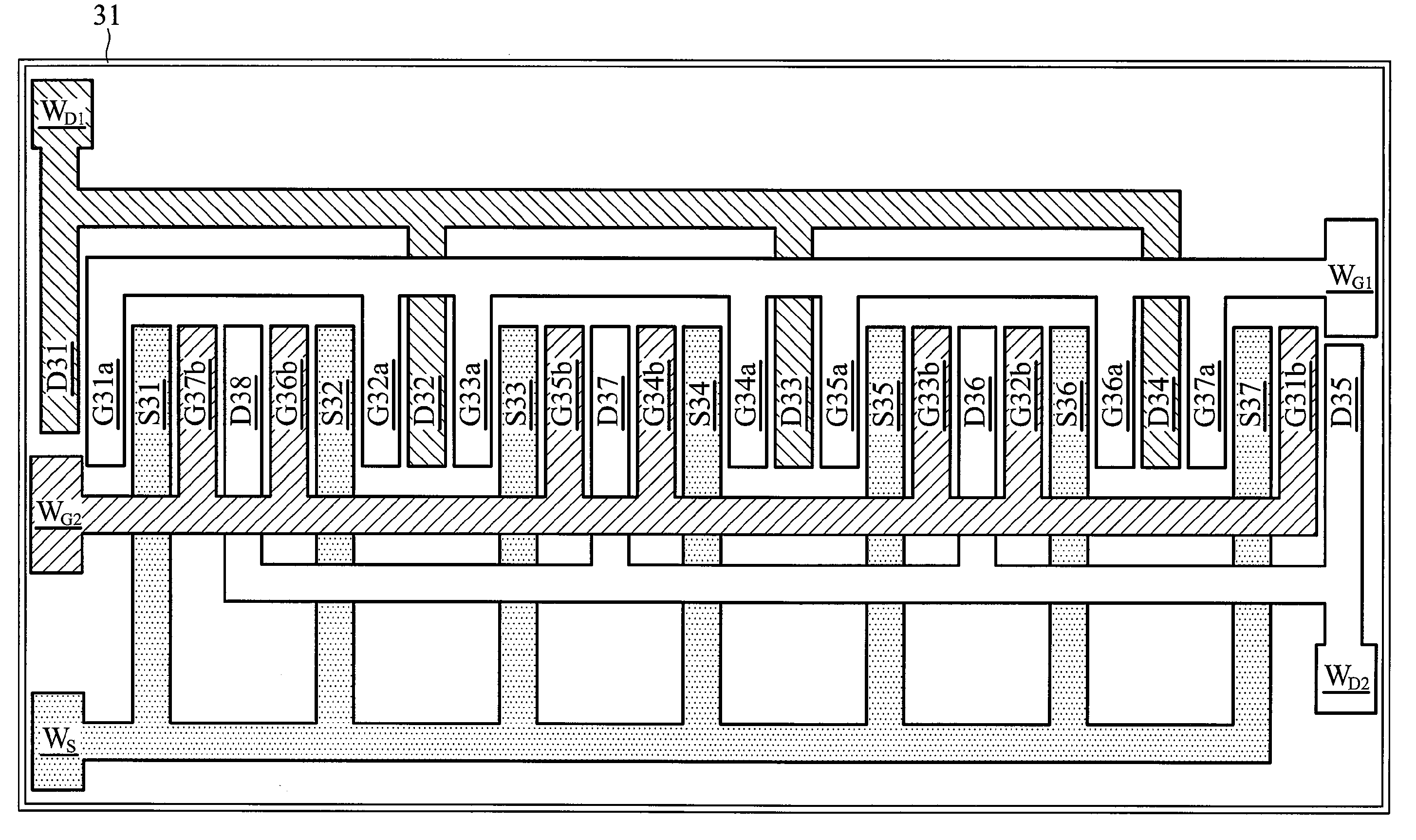
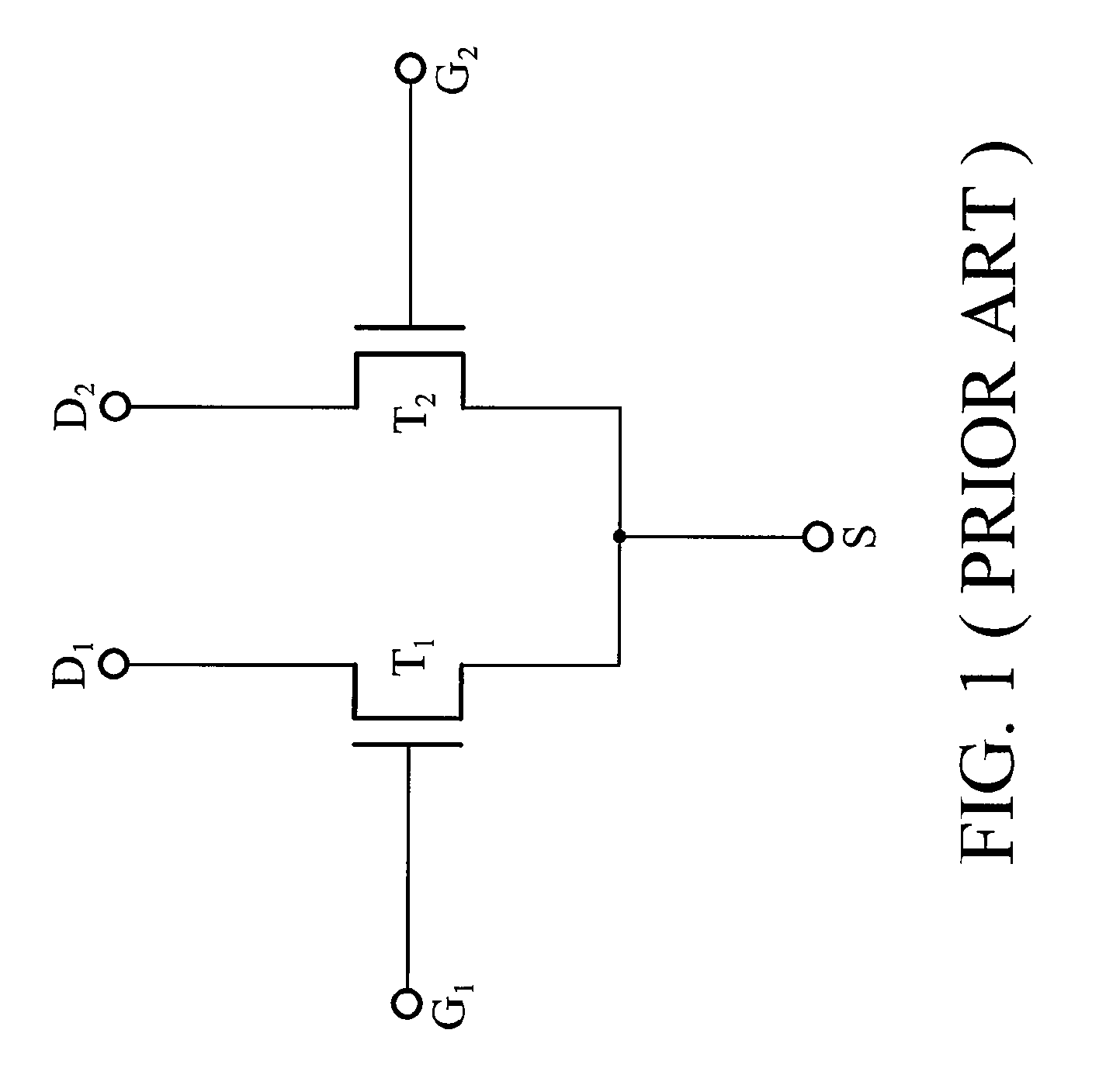
[0017]The following describes an embodiment of an integrated circuit device of the invention, with a differential pair given as an example. The differential pair relating of the invention has a circuit configuration as shown in FIG. 1, and is characterized by a circuit layout of the transistors, T1 and T2. FIG. 3 shows a circuit layout of an embodiment of the differential pair. The transistors T1 and T2 both have a multiple finger configuration. The transistor T1 has drain fingers D31 to D34 (D31, D32, D33 and D34) electrically connected to a drain wire WD1, and gate fingers G31a to G37a (G31a, G32a, G33a, G34a, G35a, G36a and G37a) electrically connected to a gate lin...


PUM


Abstract

A differential pair of an RF integrated circuit device is disclosed. The differential pair of the integrated circuit device includes a first MOS formed by a multiple finger configuration, having a plurality of first gate fingers; a second MOS formed by the multiple fingers configuration, having a plurality of second gate fingers, wherein each two first gate fingers interdigitate with each two second gate fingers.

Description

BACKGROUND OF THE INVENTION[0001]1. Field of the Invention[0002]The invention relates to an integrated circuit device, and more particularly to a differential pair configuration of an integrated circuit device for reducing layout area and parasitic capacitance.[0003]2. Description of the Related Art[0004]High-frequency integrated circuit devices are widely applied in telecommunications equipment and broadband wireless communications. The high-frequency integrated circuit devices include circuits such as a Gilbert cell. A Gilbert cell typically incorporates a differential amplification circuit and an emitter follower. A typical Gilbert cell features a circuit formed by cross-connecting two differential amplification circuits connected in series to one differential amplification circuit. FIG. 1 is a circuit diagram showing a circuit configuration of a typical differential pair. Two MOS transistors form the differential pair with a common source to multiply the difference between two i...

Claims


Application Information

Patent Timeline
Patent Type & Authority Applications(United States)
IPC IPC(8): H01L27/088
CPCH01L27/088H01L27/0207
Inventor WANG, YUJEN
Owner MEDIATEK INC
Why Eureka
Try Eureka