

Methods of fabricating semiconductor devices including channel layers having improved defect density and surface roughness characteristics
a technology of semiconductor devices and defect density, applied in semiconductor devices, semiconductor/solid-state device details, electrical devices, etc., can solve the problems of increasing the degree of integration by decreasing the size of patterns, increasing the manufacturing cost of sram devices, and reducing the number of chips manufactured on a substrate, so as to improve the surface roughness characteristics, improve the effect of quality and uniform thickness
Active Publication Date: 2008-07-03
SAMSUNG ELECTRONICS CO LTD
View PDF4 Cites 227 Cited by
- Summary
- Abstract
- Description
- Claims
- Application Information
AI Technical Summary
Benefits of technology
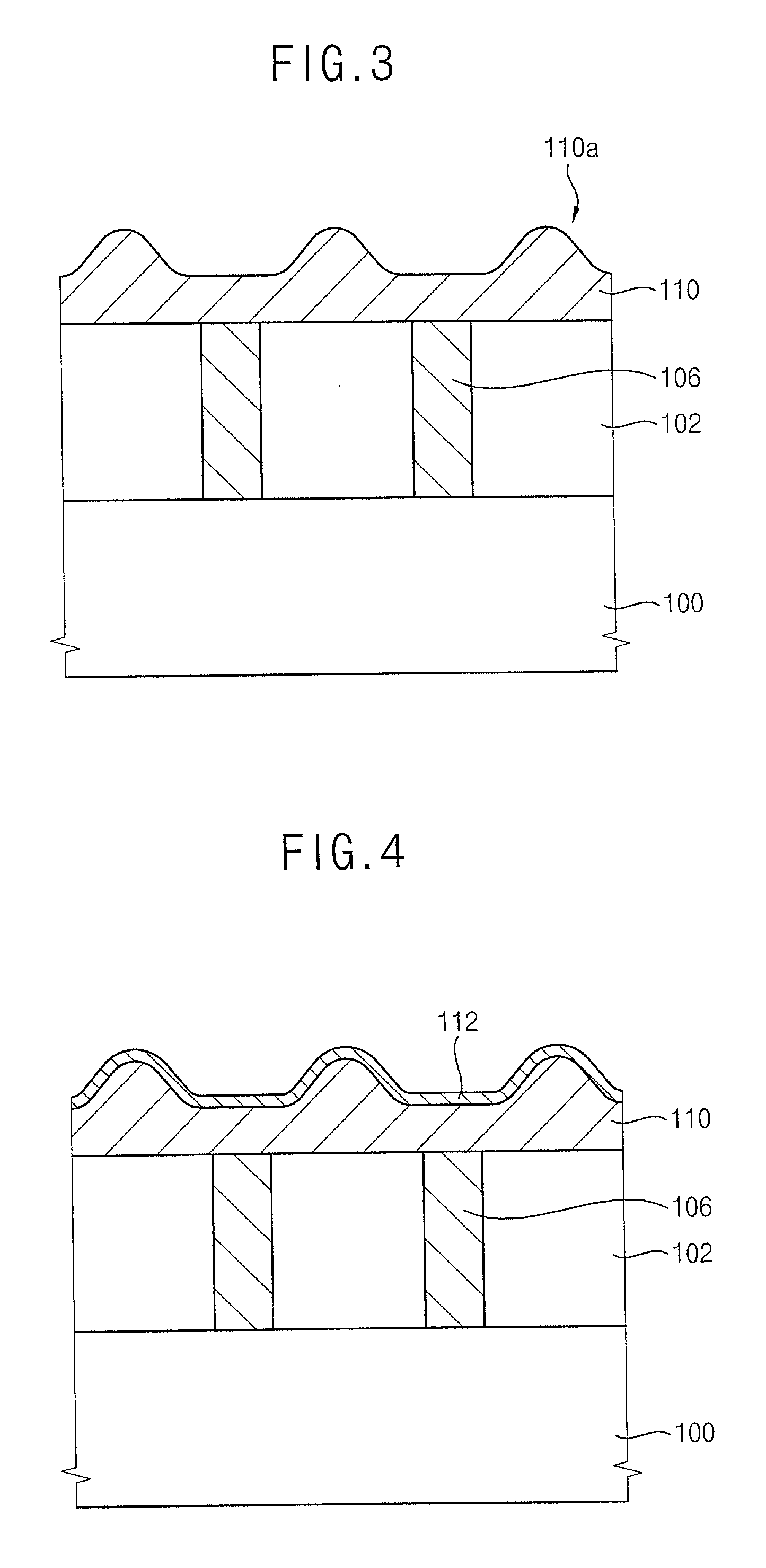
[0008]Some embodiments of the present invention provide methods of forming silicon channel layers having fewer crystal defects and improved roughness characteristics as compared to silicon channel layers formed by conventional methods. Some embodiments of the present invention also provide methods of manufacturing stacked semiconductor devices including such silicon channel layers.
[0031]Thus, according to some embodiments of the present invention, a silicon channel layer having improved surface roughness characteristics and a substantially uniform thickness may be formed even though relatively little of a relatively thin single crystalline silicon layer may be removed in polishing processes for forming the silicon channel layer. Thus, a transistor formed on the silicon channel layer may have improved characteristics, and stacked memory devices including such a transistor may have improved performance. Therefore, according to some embodiments of the present invention, a fine pattern may be simply formed using a double mask pattern and defect generation in the fine pattern may be decreased so that some embodiments of the present invention may be employed in manufacturing semiconductor devices.
Problems solved by technology
Thus, increasing the degree of integration by decreasing the sizes of the patterns may have its limits.
When the size of the cell is increased, the number of chips manufactured on a substrate may be decreased, so that the manufacturing cost of the SRAM device may be increased.
However, when the amorphous silicon layer is transformed into the single crystalline silicon layer by the thermal treatment, protrusions may be formed on an upper portion of the single crystalline silicon layer so that the single crystalline silicon layer may have relatively poor surface roughness characteristics.
However, protrusions on an upper portion of a single crystalline silicon layer may not be sufficiently removed by the method disclosed in Japanese Laid-Open Patent Publication No. 1998-106951.
Method used
View moreImage
Smart ImageViewing Examples

Examples
example 1
[0097]A silicon channel layer was formed on a substrate to have a thickness of about 29.5 nm, and a first transistor was formed on the silicon channel layer.
example 2
[0098]A silicon channel layer was formed on a substrate to have a thickness of about 25.9 nm, and a second transistor was formed on the silicon channel layer.
example 3
[0099]A silicon channel layer was formed on a substrate to have a thickness of about 19.6 nm, and a third transistor was formed on the silicon channel layer.
Login to View More PUM
 Abstract
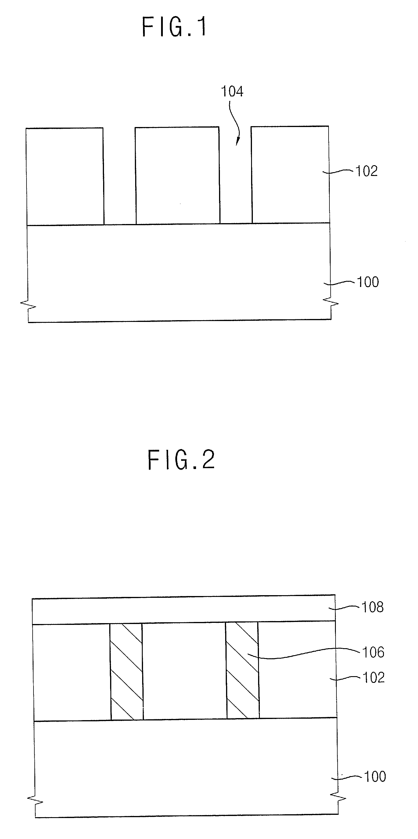
A method of fabricating a semiconductor device including a channel layer includes forming a single crystalline semiconductor layer on a semiconductor substrate. The single crystalline semiconductor layer includes a protrusion extending from a surface thereof. A first polishing process is performed on the single crystalline semiconductor layer to remove a portion of the protrusion such that the single crystalline semiconductor layer includes a remaining portion of the protrusion. A second polishing process different from the first polishing process is performed to remove the remaining portion of the protrusion and define a substantially planar single crystalline semiconductor layer having a substantially uniform thickness. A sacrificial layer may be formed on the single crystalline semiconductor layer and used as a polish stop for the first polishing process to define a sacrificial layer pattern, which may be removed prior to the second polishing process. Related methods of fabricating stacked semiconductor memory devices are also discussed.
Description
CROSS-REFERENCE TO RELATED APPLICATIONS[0001]This application claims priority under 35 USC §119 to Korean Patent Application No. 10-2006-0134399, filed on Dec. 27, 2006 in the Korean Intellectual Property Office (KIPO), the disclosure of which is incorporated by reference herein in its entirety.FIELD OF THE INVENTION[0002]The present invention relates to semiconductor devices, and more particularly, to methods of forming channel layers in semiconductor devices.BACKGROUND OF THE INVENTION[0003]In semiconductor devices, sizes of patterns formed on a chip and / or distances between adjacent patterns may be decreased in order to realize higher degrees of integration. When the sizes of the patterns are decreased, the patterns may have an increased resistance. Thus, increasing the degree of integration by decreasing the sizes of the patterns may have its limits. Accordingly, instead of decreasing the sizes of the patterns, stacked semiconductor devices in which unit elements (such as metal-...
Claims
Login to View More Application Information
Patent Timeline
 Patent Type & AuthorityApplications(United States)
IPC IPC(8): H01L21/20
CPCH01L21/02381H01L21/02532H01L29/78H01L21/02636H01L21/02675H01L21/0262H01L21/18H01L23/12
InventorLIM, JONG HEUNHONG, CHANG-KIYOON, BO-UNYUN, SEONG-KYUCHOI, SUK-HUNHAN, SANG-YEOB
OwnerSAMSUNG ELECTRONICS CO LTD