Thermal treatment of a semiconductor layer

a technology of thermal treatment and semiconductor layer, which is applied in the direction of semiconductor/solid-state device manufacturing, basic electric elements, electric devices, etc., can solve the problems of defective zone having to be completely removed, costing and complex treatment steps, and affecting the crystalline quality so as to improve the crystalline quality and surface roughness of the transfer layer, improve the effect of surface roughness and good crystalline quality

Active Publication Date: 2007-10-16
SOITEC SA
View PDF55 Cites 8 Cited by
  • Summary
  • Abstract
  • Description
  • Claims
  • Application Information

AI Technical Summary

Benefits of technology

[0015]The present invention is directed to methods for forming a semiconductor structure that includes a transfer layer having a good crystalline quality and an improved surface roughness characteristic. An embodiment of the technique includes co-implanting atomic species into a first surface of a donor wafer of a silicon germanium semiconductor material to form a zone of weakness therein at a predetermined depth that defines the thickness of a transfer layer; bonding the first surface of the donor wafer to a host wafer; supplying energy to detach the transfer layer from the donor wafer at the zone of weakness; and conducting a recovery operation that includes heat treating the transfer layer after detachment, but while the layer remains in contact with the donor wafer, for a predetermined duration at a recovery temperature that is lower than a re-adhesion temperature at which the transfer layer would re-adhere to the donor wafer, to improve crystalline quality and surface roughness of the transfer layer.

Problems solved by technology

Such a treatment step for the transferred layer 1 is costly and complex.
The defective zone has to be completely removed after detachment, in particular due to the defects present within the transfer layer.
Such a treatment step of the transfer layer 1 is consequently costly and complex from an economic point of view.
This results in a loss of time, extra wafer handling and the need to use suitable equipment.
However, selective etching is imprecise, and thus a roughness remains at the tip or edge of the first chemical etching step which is at the interface between the defective zone 1A and the stop layer.
However, the combination of polishing and selective etching further adds to the complexity and cost of the operation, which could make the overall operation unprofitable.
A similar problem exists here analogous to that discussed above, wherein the surface of sound zone 1B is unequally etched because the tip of the etching portion reached it.
In other words, a compromise has to be made between roughness and formation of these defects, and the recourse to co-implantation thus does not allow as such to satisfactorily solve the above mentioned problems relating to the presence of defects and a superficial roughness.

Method used


Image

  • Thermal treatment of a semiconductor layer
  • Thermal treatment of a semiconductor layer
  • Thermal treatment of a semiconductor layer

Examples


Embodiment Construction

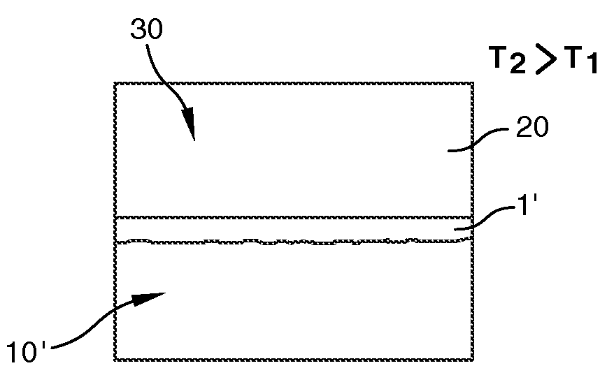
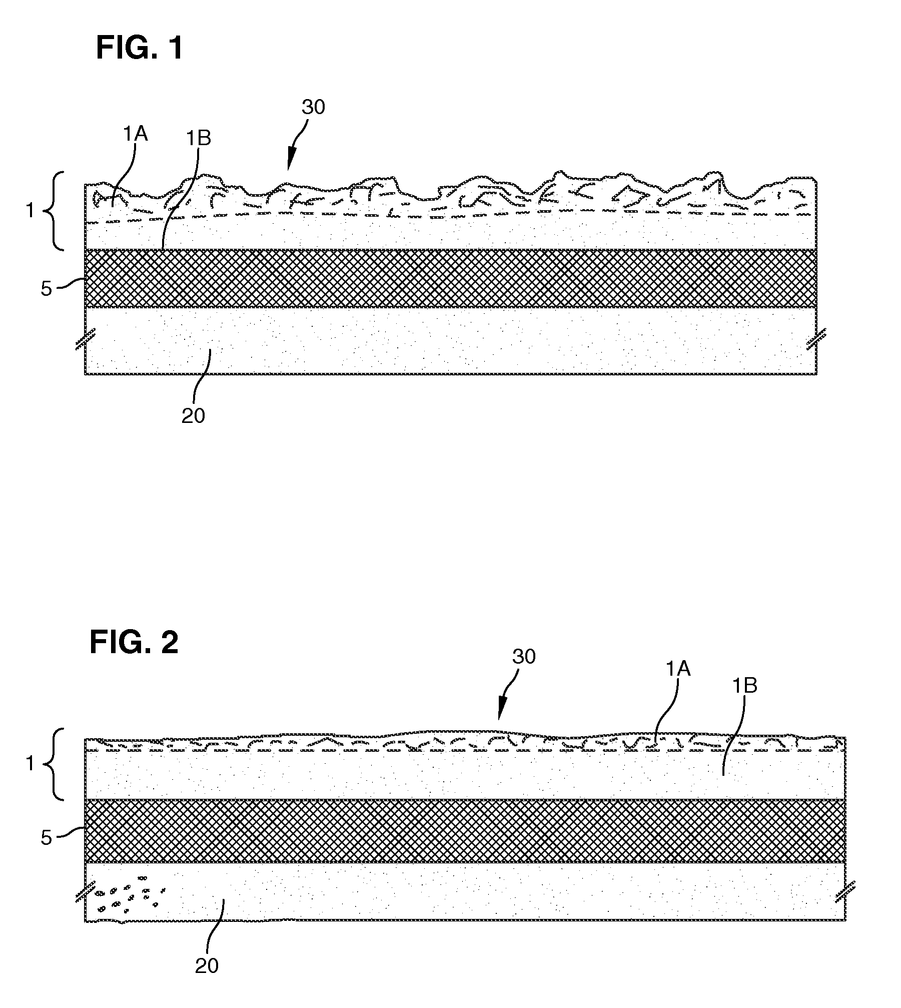
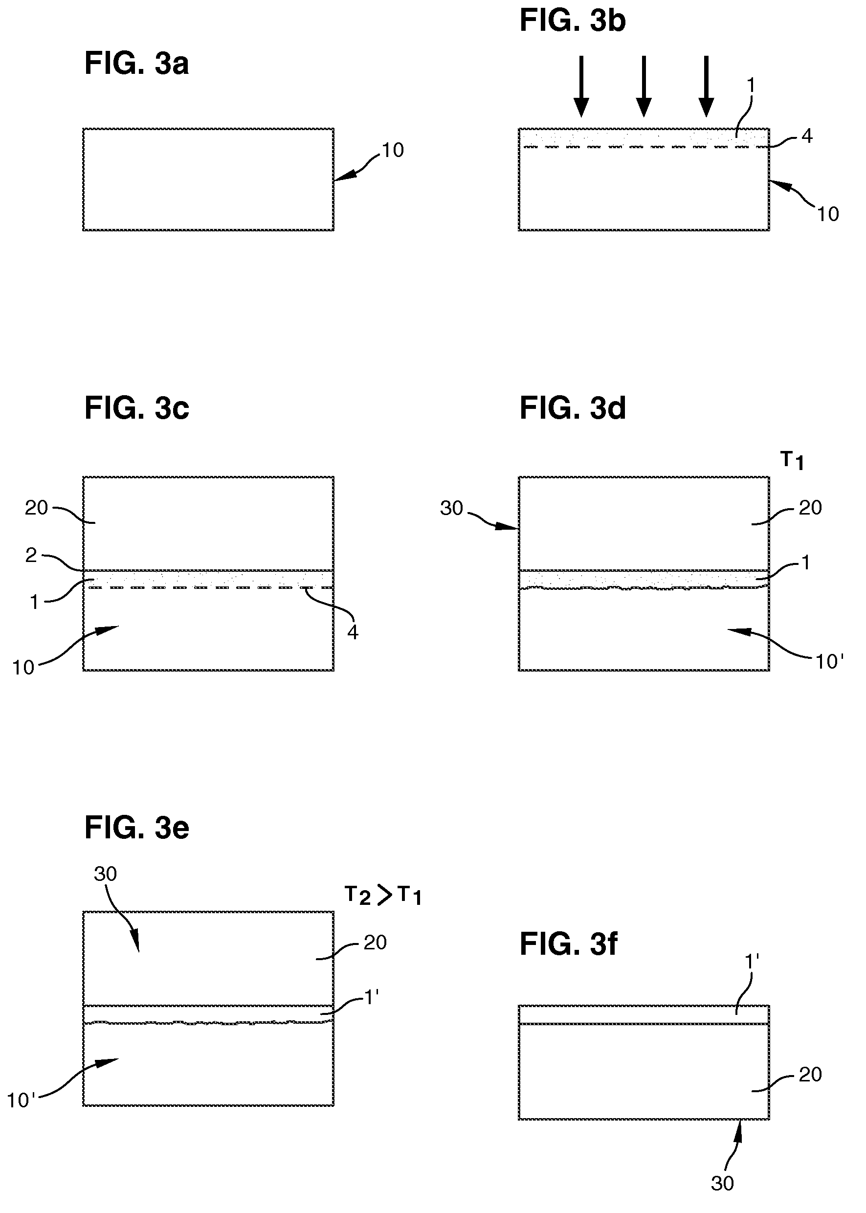
[0029]The invention advantageously reduces the duration, economic cost and number of treatment devices required for transferring a layer using the SMART-CUT® process. In addition, the method provides a simple way to treat a transfer layer that is easy to incorporate into the SMART-CUT® process, and provides a way to use a recovery heat treatment for the transfer layer both in inert atmosphere and in oxidizing atmosphere without substantially altering the properties of the transfer layer. Further, the method according to the invention improves the crystalline quality of the transfer layer, and makes it possible to produce semiconductor on insulator structures with high crystalline quality and a working layer thickness that can be very thin. The method also reduces the quantity of material removed during treatment of the transfer layer using the SMART-CUT® process. Lastly, the method according to the invention makes it possible to utilize SiGe or Ge for fabricating a semiconductor on ...


PUM


Abstract

A method for thermally treating a silicon germanium semiconductor layer from a donor wafer is described. An embodiment of the technique includes co-implanting atomic species into a first surface of the donor wafer to form a zone of weakness at a predetermined depth that defines the thickness of a transfer layer, bonding the first surface of the donor wafer to a host wafer, supplying energy to detach the transfer layer from the donor wafer at the zone of weakness, and conducting a recovery operation on the transfer layer. The recovery operation is conducted after detachment but while the layer remains in contact with the donor wafer. The recovery operation includes heat treating the transfer layer for a predetermined duration at a recovery temperature that is lower than a re-adhesion temperature at which the transfer layer would re-adhere to the donor wafer, to improve the crystalline quality and the surface roughness of the transfer layer. The co-implanting step preferably includes implanting hydrogen and helium.

Description

CROSS-REFERENCE TO RELATED APPLICATIONS[0001]This application is a continuation of International application PCT / FR2005 / 000543 filed Mar. 7, 2005, and a continuation-in-part of application Ser. No. 11 / 058,992 filed Feb. 16, 2005, the entire content of each of which is expressly incorporated herein by reference thereto.FIELD OF THE INVENTION[0002]The invention relates to methods for forming a semiconductor structure that includes a transfer layer taken from a donor wafer. The techniques include implanting atomic species to form a zone of weakness zone in the donor wafer that defines a transfer layer, bonding the donor wafer to a host wafer, supplying energy to detach the transfer layer from the donor wafer at the zone of weakness zone, and treating the transfer layer.BACKGROUND ART[0003]A semiconductor layer transfer method called SMART-CUT® is known to those skilled in the art. Details of this method may be found in many published documents, for example, on pages 50 and 51 of: “Sili...

Claims


Application Information

Patent Timeline
Patent Type & Authority Patents(United States)
IPC IPC(8): H01L21/302
CPCH01L21/26506
Inventor DAVAL, NICOLASAKATSU, TAKESHINGUYEN, NGUYET-PHUONG
Owner SOITEC SA
Why Eureka
Try Eureka