

Piezoelectric thin film resonator, piezoelectric thin film resonator filter and manufacturing method thereof
a piezoelectric thin film and filter technology, applied in the direction of instruments, device material selection, device details, etc., can solve the problems of piezoelectric thin film bulk acoustic wave resonators, adverse effect on element characteristics, etc., and achieve good film quality characteristics and prevent the effect of oxidation of each thin film
- Summary
- Abstract
- Description
- Claims
- Application Information
AI Technical Summary
Benefits of technology
Problems solved by technology
Method used
Image

Examples
first embodiment
[0038]A first embodiment of a piezoelectric thin film bulk acoustic wave resonator according to the present invention will be described with reference to FIGS. 1A to 6.
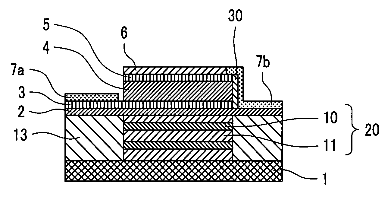
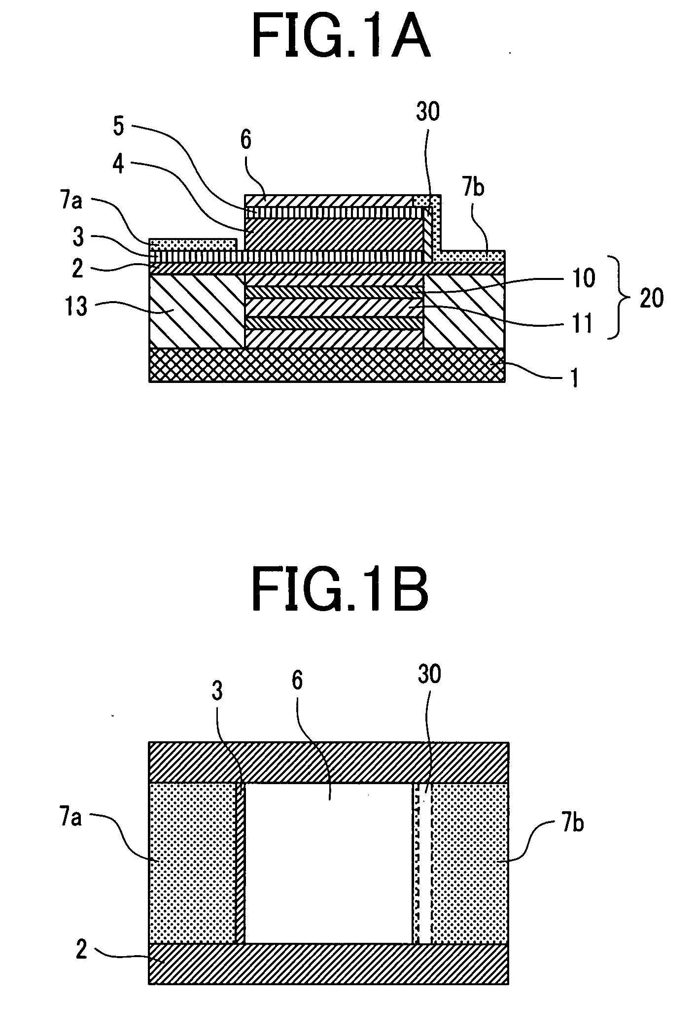
[0039]First, a structure of the piezoelectric thin film bulk acoustic wave resonator according to the first embodiment will be described with reference to FIG. 1A and FIG. 1B. FIG. 1A is a longitudinal sectional structured view of the piezoelectric thin film bulk acoustic wave resonator according to the first embodiment. FIG. 1B is a top view of the piezoelectric thin film bulk acoustic wave resonator shown in FIG. 1A.
[0040]The piezoelectric thin film bulk acoustic wave resonator according to the first embodiment includes: a support film 2 made of AlN on an acoustic insulating layer 20 produced on an insulating substrate 1; and a laminated structure, on the support film 2, which has a piezoelectric thin film 4, and a first metal electrode film 3 and a second metal electrode film 5 that interpose at least a part of the...
second embodiment
[0065]FIG. 6 is a sectional structured view showing one example of a piezoelectric thin film bulk acoustic wave resonator of a second embodiment according to the present invention. The second embodiment is characterized in that a laminated structure which includes a piezoelectric thin film 4, and a first metal electrode film 3 and a second metal electrode film 5 that interpose at least a part of the piezoelectric thin film 4 is produced, and an AlN thin film is formed as a protection film 6 so as to cover the second metal electrode film 5 which serves as an upper electrode.
[0066]At this time, a support film 2, the first metal electrode film 3, the piezoelectric thin film 4, the second metal electrode film 5, and the protection film 6 made of AlN are sequentially deposited in vacuum, so that deterioration of film quality due to oxidization of each thin film can be prevented to the minimum degree. Therefore, the piezoelectric thin film bulk acoustic wave resonator with a good characte...
third embodiment
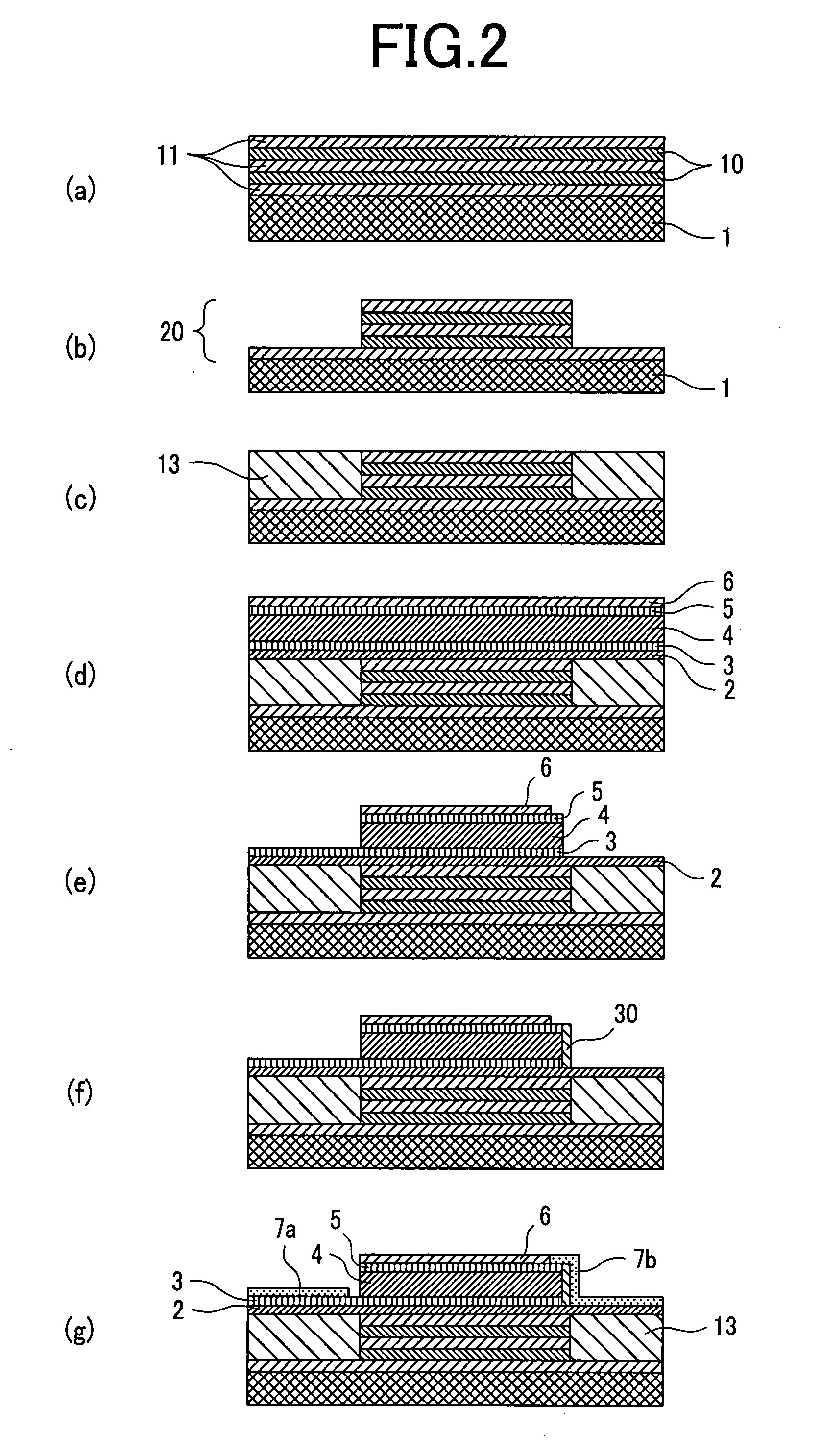
[0076]FIG. 8A to FIG. 8F show one example of a manufacturing method of a piezoelectric thin film bulk acoustic wave resonator of a third embodiment according to the present invention. First, a cavity 60 having a depth of 800 nm is provided on a high-resistance silicon substrate 1 as an insulating substrate by an ordinary photoresist process and an ordinary etching process. Next, a barrier layer 40 made of Si3N4 is deposited so as to have a thickness of 100 nm on a surface of the insulating substrate 1 where the cavity 60 is formed, and further, a sacrificial layer 50 made of phosphoric-silicate glass (PSG) is deposited so as to have a thickness of 1000 nm. (Step a)
[0077]Next, the sacrificial layer 50 is made flat by a chemical mechanical polishing method (CMP) in such a manner that a surface of the barrier layer 40 formed on the insulating substrate 1 is exposed, and only the cavity 60 is filled with the sacrificial layer 50. (Step b)
[0078]Next, on the insulating substrate 1 in whic...
PUM
| Property | Measurement | Unit |
|---|---|---|
| Thickness | aaaaa | aaaaa |
| Thickness | aaaaa | aaaaa |
| Piezoelectricity | aaaaa | aaaaa |
Abstract
Description
Claims
Application Information