Circuit Structure with Low Dielectric Constant Regions and Method of Forming Same

a circuit structure and dielectric constant technology, applied in the field of circuit structures, can solve the problems of difficult integration of porous materials with other beol module processes, low mechanical properties of most porous materials, and inability to offer reasonable coverage on the surface of porous dielectrics by physical vapor deposition (pvd) diffusion barrier deposition technology, etc., to achieve low dielectric constant and reduce parasitic capacitance

Inactive Publication Date: 2008-07-17
ELPIS TECH INC
View PDF8 Cites 20 Cited by
  • Summary
  • Abstract
  • Description
  • Claims
  • Application Information

AI Technical Summary

Benefits of technology

[0010]Principles of the present invention provide techniques for forming circuit structures with low dielectric constant regions. An exemplary embodiment of a method for manufacturing a circuit, according to one aspect of the invention, includes the step of providing a first wiring level comprising first wiring level conductors separated by a first wiring level dielectric material. Further, a first dielectric layer of first dielectric layer material is formed above the first wiring level, the first dielectric layer having a plurality of interconnect openings and a plurality of gap openings. The interconnect openings and the gap openings are pinched off with a pinching dielectric material to form relatively low dielectric constant (low-k) volumes in the gap openings. Metallic conductors comprising second wiring level conductors, and interconnects are formed at the interconnect openings while maintaining the relatively low-k volumes in the gap openings. The first wiring level conductors, the second wiring level conductors, and the interconnects form a series of conductor structures. The gap openings with the relatively low-k volumes reduce parasitic capacitance between adjacent ones of the conductor structures as compared to an otherwise comparable circuit not including the gap openings with the relatively low-k volumes.

Problems solved by technology

Lowering parasitic capacitance can be achieved with new porous low k dielectrics, however most of the porous materials have relatively weak mechanical properties as compared to dense dielectrics.
It is also difficult to integrate these materials with other BEOL module processes.
For example, the conventional chemical-mechanical polish process has difficulty in polishing porous dielectric, and the conventional physical vapor deposition (PVD) diffusion barrier deposition technology cannot offer reasonable coverage on the surface of porous dielectrics.
Current art references directed to forming air dielectrics for microelectronic applications do not set forth techniques that can be employed in practical manufacturing processes.
The resulting structure is very unstable and cannot sustain any mechanical stress.
For example, the structure cannot be further processed by employing a chemical-mechanical polishing process.
It is not compatible with any existing packaging methodology.
Randomly removing dielectric substances and replacing them with air cannot be implemented in the current manufacturing environment.
Trapping of residual chemicals will cause yield and reliability failure, and the weak structure literally cannot protect the metallization levels of the chip.
The added complexity increase costs and subjects the process to significantly increased process time per metal level.

Method used


Image

  • Circuit Structure with Low Dielectric Constant Regions and Method of Forming Same
  • Circuit Structure with Low Dielectric Constant Regions and Method of Forming Same
  • Circuit Structure with Low Dielectric Constant Regions and Method of Forming Same

Examples


Embodiment Construction

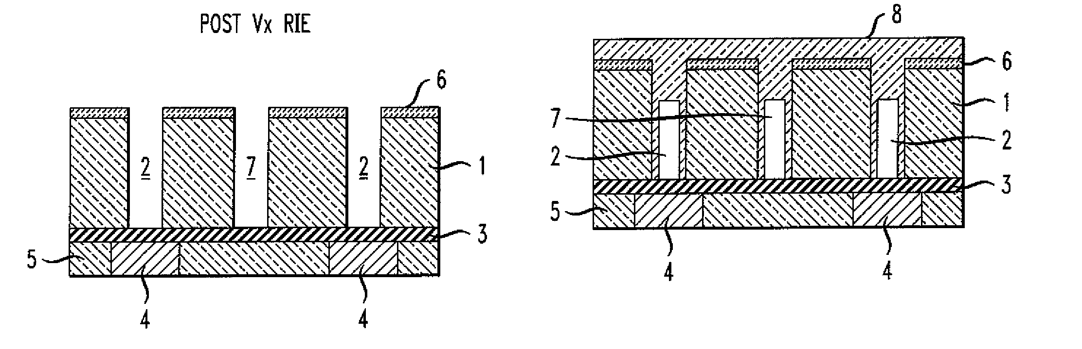
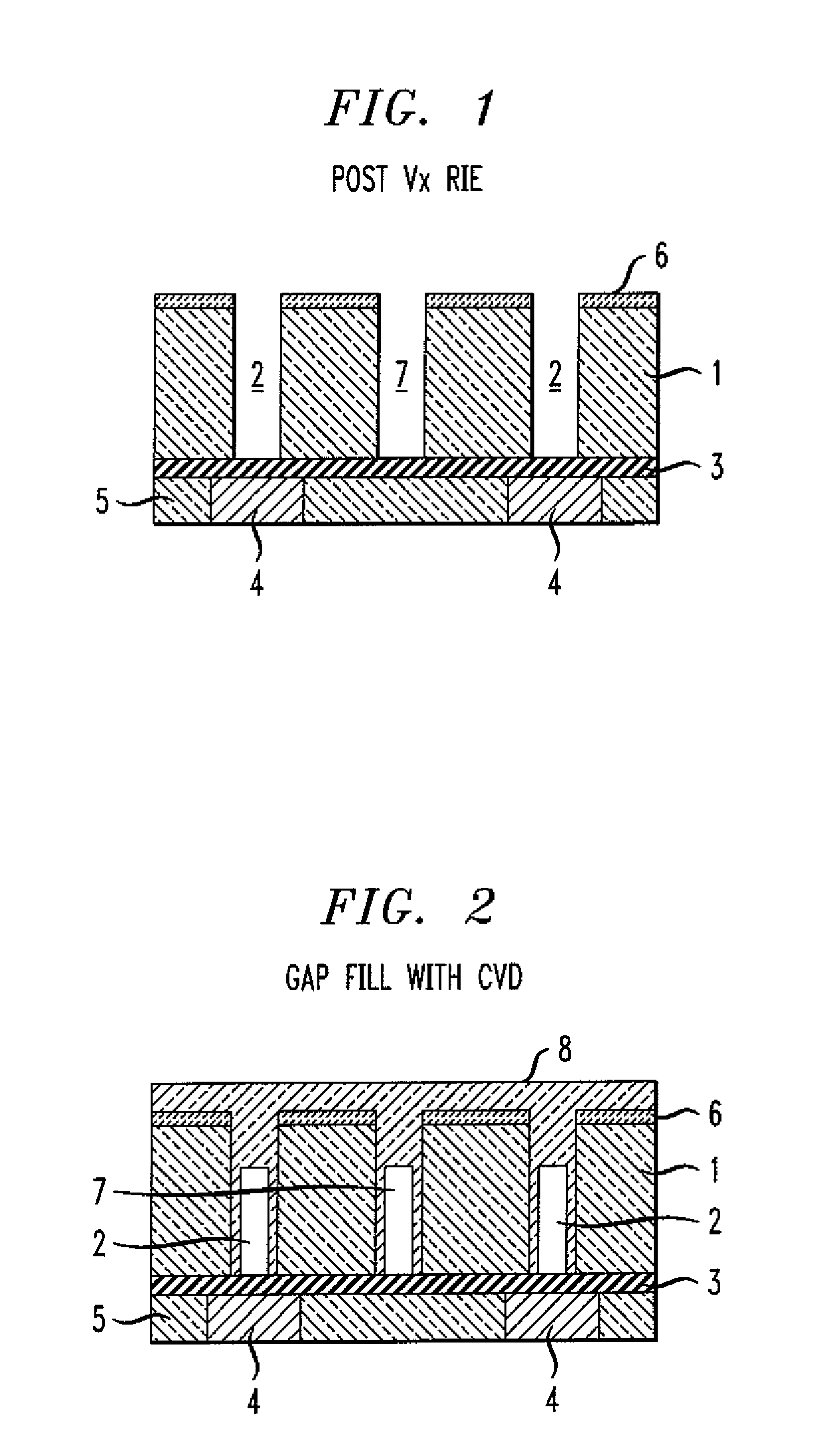
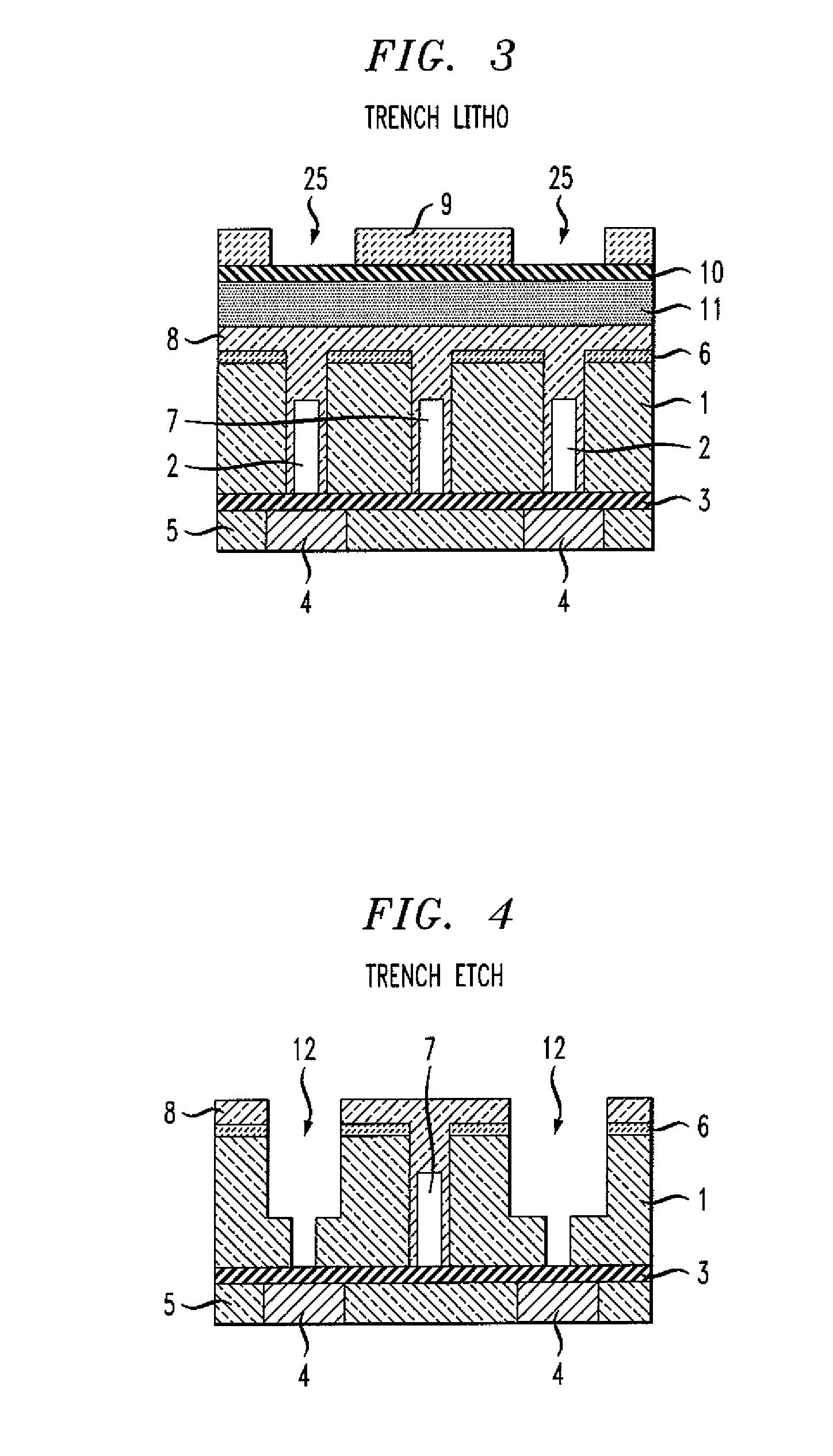
[0015]An exemplary method of manufacturing a circuit (such as a microelectronic circuit) will now be described with respect to the figures, in which like reference characters are used throughout to refer to like elements, unless otherwise noted. With reference to FIG. 1, which is a cross-sectional view (as are FIGS. 1-6), one step of the method includes providing a first wiring level comprising first wiring level conductors 4 separated by a first wiring level dielectric material 5. A first dielectric layer 1 of first dielectric layer material is formed above the first wiring level, the first dielectric layer 1 having a plurality of interconnect openings 2 and a plurality of gap openings 7. Optionally, a capping layer 3 can be formed over the first wiring level prior to forming the first dielectric layer, and also, a capping layer 6 can optionally be formed over the first dielectric level. Note that interconnect openings 2 are formed over conductors 4, while gap openings 7 are not. T...


PUM


Abstract

A method for manufacturing a circuit includes the step of providing a first wiring level comprising first wiring level conductors separated by a first wiring level dielectric material. A first dielectric layer with a plurality of inter connect openings and a plurality of gap openings is formed above the first wiring level. The interconnect openings and the gap openings are pinched off with a pinching dielectric material to form relatively low dielectric constant (low-k) volumes in the gap openings. Metallic conductors comprising second wiring level conductors and interconnects to the first wiring level conductors are formed at the interconnect openings while maintaining the relatively low-k volumes in the gap openings. The gap openings with the relatively low-k volumes reduce parasitic capacitance between adjacent conductor structures formed by the conductors and interconnects.

Description

FIELD OF THE INVENTION[0001]The present invention generally relates to the electrical and electronic arts and, more particularly, to circuit structures and their formation.BACKGROUND OF THE INVENTION[0002]To minimize the back-end-of-line (BEOL) interconnect portion of circuit delay, the conventional SiO2 dielectric (dielectric constant, k˜4.0) has been replaced with dense lower-k films (k<3.0). For further performance improvement, more parasitic capacitance reduction is required (k<2.5) for high-speed circuits.[0003]Lowering parasitic capacitance can be achieved with new porous low k dielectrics, however most of the porous materials have relatively weak mechanical properties as compared to dense dielectrics. It is also difficult to integrate these materials with other BEOL module processes. For example, the conventional chemical-mechanical polish process has difficulty in polishing porous dielectric, and the conventional physical vapor deposition (PVD) diffusion barrier deposi...

Claims


Application Information

Patent Timeline
Patent Type & Authority Applications(United States)
IPC IPC(8): H01L21/4763
CPCH01L21/7682H01L21/76808
Inventor CLEVENGER, LAWRENCE A.COLBURN, MATTHEW E.HSU, LOUIS C.LI, WAI-KIN
Owner ELPIS TECH INC
Why Eureka
Try Eureka