Plasma processing apparatus component and manufacturing method thereof
- Summary
- Abstract
- Description
- Claims
- Application Information
AI Technical Summary
Benefits of technology
Problems solved by technology
Method used
Image

Examples
Embodiment Construction
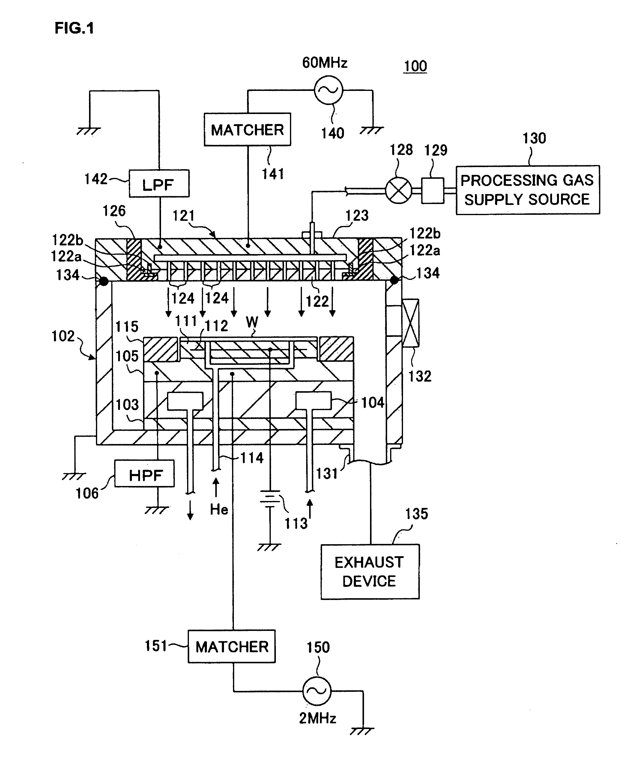
[0034]The following is a detailed explanation of a preferred embodiment of a plasma processing apparatus component and a manufacturing method thereof according to the present invention, given in reference to the attached drawings. A plasma processing apparatus that may include a component achieved in the embodiment is first described. FIG. 1 is a sectional view showing an example of a structure that may be adopted in the plasma processing apparatus. The explanation is provided by assuming that the plasma processing apparatus is a plane-parallel plasma etching apparatus.
(Specific Example of Plasma Processing Apparatus)
[0035]A plasma processing apparatus 100 includes a processing chamber 102 constituted of an electrically conductive material such as aluminum, a lower electrode (susceptor) 105 disposed on the bottom surface within the processing chamber 102, on which a wafer W (i.e., the processing target substrate) is placed, and an upper electrode 121 disposed so as to face opposite ...
PUM
| Property | Measurement | Unit |
|---|---|---|
| Shape | aaaaa | aaaaa |
| Energy | aaaaa | aaaaa |
Abstract
Description
Claims
Application Information
 - Generate Ideas
- Intellectual Property
- Life Sciences
- Materials
- Tech Scout
- Unparalleled Data Quality
- Higher Quality Content
- 60% Fewer Hallucinations
Browse by: Latest US Patents, China's latest patents, Technical Efficacy Thesaurus, Application Domain, Technology Topic, Popular Technical Reports.
© 2025 PatSnap. All rights reserved.Legal|Privacy policy|Modern Slavery Act Transparency Statement|Sitemap|About US| Contact US: help@patsnap.com