Semiconductor memory and method for manufacturing the same

a technology of semiconductor devices and memory, applied in the field of semiconductor memory, can solve the problems of increasing the cost with an increase in the number of stacks, not being able to circumvent the minimum design rule, and becoming difficult to reduce the minimum design rul

Active Publication Date: 2008-07-24
KIOXIA CORP
View PDF12 Cites 502 Cited by
  • Summary
  • Abstract
  • Description
  • Claims
  • Application Information

AI Technical Summary

Benefits of technology

[0009]According to an aspect of the present invention, there is provided a nonvolatile semiconductor memory including: a plurality of memory devices each having: a resistance change element, and a diode connected serially to the resistance change element; and a source conductive layer spreading two-dimensionally to be connected to one ends of the plurality of memory devices.

Problems solved by technology

To realize further micromachining of wiring patterns, etc., very advanced machining technique is required and therefore it becomes difficult to reduce the minimum design rule.
In most of the semiconductor memories in the related arts each with memory cells placed three-dimensionally, the memory cells are stacked simply and an increase in the cost with an increase in the number of stacks is not circumvented.

Method used


Image

  • Semiconductor memory and method for manufacturing the same
  • Semiconductor memory and method for manufacturing the same
  • Semiconductor memory and method for manufacturing the same

Examples


first embodiment

(Nonvolatile Semiconductor Memory 1 of Unipolar Operation)

(OxReRAM: Oxide Resistive RAM)

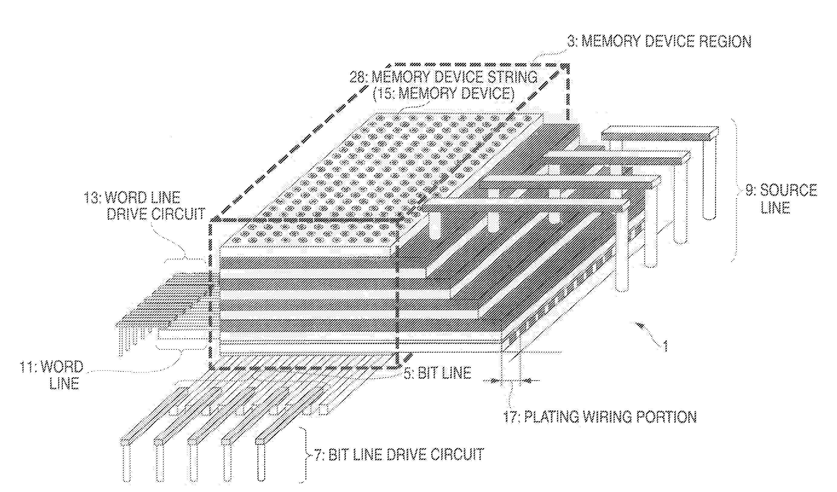
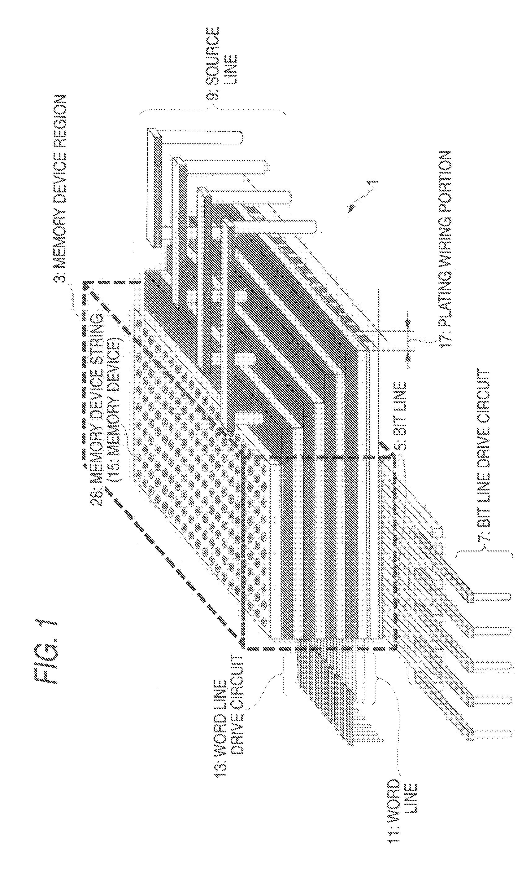
[0104]FIG. 1 shows the schematic configuration of a nonvolatile semiconductor memory 1 according to a first embodiment. The nonvolatile semiconductor memory 1 has a memory device region 3, bit lines 5, a bit line drive circuit 7, source lines 9, word lines 11, a word line drive circuit 13, etc. A plating wiring portion 17 of the nonvolatile semiconductor memory 1 according to the first embodiment indicates a portion cut after a plating process of the nonvolatile semiconductor memory 1. As shown in FIG. 1, in the nonvolatile semiconductor memory 1, memory devices 15 forming the memory device region 3 are formed by stacking semiconductor layers. As shown in FIG. 1, the source lines 9 of each layer are spread two-dimensionally. The source lines 9 of each layer have a plate-like flat structure made of the same layer. In the nonvolatile semiconductor memory 1, the direction of current flowing into the...

third embodiment

(Manufacturing Process of Nonvolatile Semiconductor Memory of Unipolar Operation)

(OxReRAM: Oxide Resistive RAM)

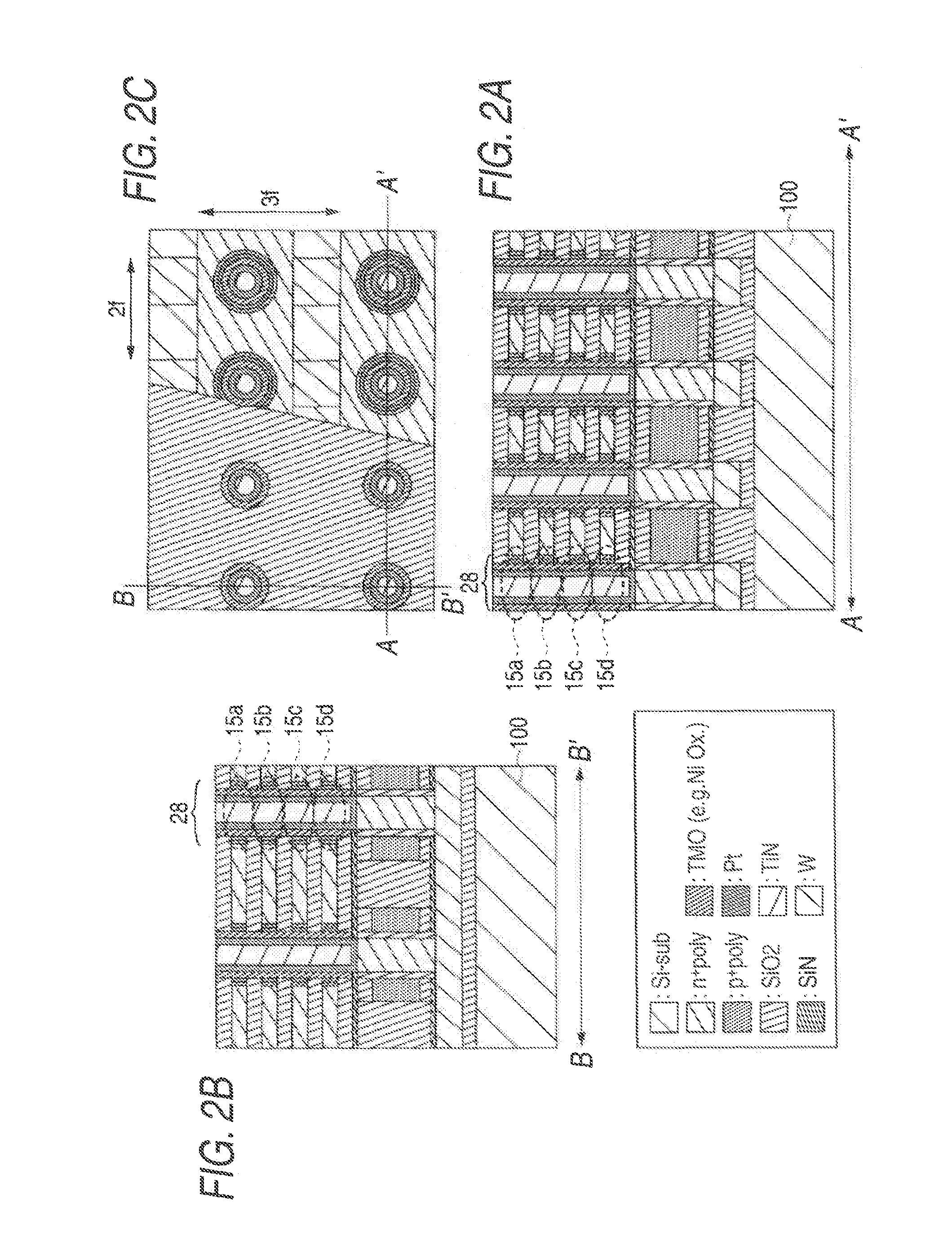
[0182]A manufacturing process of nonvolatile semiconductor memory 1 according to a third embodiment will be discussed with reference to FIGS. 41A to 48C. In the embodiment, to form a resistance change element forming a part of a memory device 15, the surface of a titanium nitride (TiN) silicide forming the resistance change element is oxidized. In the embodiment, plating wiring need not be formed because a plating process as described in the first embodiment is not required.

[0183]FIGS. 41A to 48C show each a part of the memory device region 3 of the nonvolatile semiconductor memory 1 according to the third embodiment as in the first embodiment. FIGS. 41C to 48C are top views of the memory device region 3. FIGS. 41A to 48A are sectional views of the memory device region 3 taken on line A-A′ in FIGS. 41C to 48C. FIGS. 41B to 48B are sectional views of the memory device region...

fourth embodiment

(PRAM: Phase Change RAM)

[0196]In a fourth embodiment, a nonvolatile semiconductor memory of phase change type using a phase change film of GST (GeSbTe), etc., (PRAM: Phase Change RAM) will be discussed as an example of nonvolatile semiconductor memory of unipolar operation.

[0197]FIG. 49 shows the schematic configuration of a nonvolatile semiconductor memory 200 according to the fourth embodiment. The nonvolatile semiconductor memory 200 according to the fourth embodiment has a memory device region 3, bit lines 5, a bit line drive circuit 7, source lines 9, word lines 11, a word line drive circuit 13, etc. A plating wiring portion 17 of the nonvolatile semiconductor memory 200 according to the fourth embodiment indicates a portion cut after a plating process performed in manufacturing the nonvolatile semiconductor memory 200. As shown in FIG. 49, in the nonvolatile semiconductor memory 200, memory devices 15 forming the memory device region 3 are formed by stacking semiconductor laye...


PUM


Abstract

According to an aspect of the present invention, there is provided a nonvolatile semiconductor memory including: a plurality of memory devices each having: a resistance change element, and a diode connected serially to the resistance change element; and a source conductive layer spreading two-dimensionally to be connected to one ends of the plurality of memory devices.

Description

CROSS-REFERENCE TO RELATED APPLICATIONS[0001]The entire disclosure of Japanese Patent Application No. 2007-013163 filed on Jan. 23, 2007 including specification, claims, drawings and abstract is incorporated herein by reference in its entirety.BACKGROUND OF THE INVENTION[0002]1. Field of the Invention[0003]An aspect of the present invention relates to semiconductor memory wherein data can be electrically rewritten and a manufacturing method thereof.[0004]2. Description of the Related Art[0005]To advance higher integration and larger capacity of semiconductor memory, the minimum design rule needs to be reduced. To reduce the minimum design rule, further micromachining of wiring patterns, etc., becomes necessary. To realize further micromachining of wiring patterns, etc., very advanced machining technique is required and therefore it becomes difficult to reduce the minimum design rule.[0006]In recent years, to enhance the integration degree of memory, a large number of semiconductor m...

Claims


Application Information

Patent Timeline
Patent Type & Authority Applications(United States)
IPC IPC(8): G11C5/02G11C5/06
CPCG11C5/025H01L45/147G11C11/16G11C13/0007G11C13/0023G11C13/0026G11C13/0028G11C2213/31G11C2213/32G11C2213/71G11C2213/72H01L27/101H01L27/224H01L27/228H01L27/2409H01L27/2454H01L27/249H01L45/06H01L45/085H01L45/1226H01L45/144G11C5/063G11C11/1655G11C11/1659H10B61/10H10B63/34H10B63/845H10B63/20H10B61/22H10N70/245H10N70/823H10N70/231H10N70/8836H10N70/8828
Inventor TANAKA, HIROYASUKATSUMATA, RYOTAAOCHI, HIDEAKIKIDOH, MASARUKITO, MASARUSATO, MITSURU
Owner KIOXIA CORP
Why Eureka
Try Eureka