Resin Film Substrate for Organic Electroluminescence and Organic Electroluminescence Device

Inactive Publication Date: 2008-07-24
KONICA MINOLTA INC
View PDF2 Cites 81 Cited by
  • Summary
  • Abstract
  • Description
  • Claims
  • Application Information

AI Technical Summary

Benefits of technology

[0018]The present invention provides a low cost resin film substrate for organic electroluminescence comprising a gas barrier which has high gas barrier properties and

Problems solved by technology

In organic electroluminescence using a film substrate (also called organic EL hereinafter) light emitting device, there is a problem in that the light taking-out efficiency is low.
There are problems

Method used


Image

  • Resin Film Substrate for Organic Electroluminescence and Organic Electroluminescence Device
  • Resin Film Substrate for Organic Electroluminescence and Organic Electroluminescence Device
  • Resin Film Substrate for Organic Electroluminescence and Organic Electroluminescence Device

Examples


second embodiment

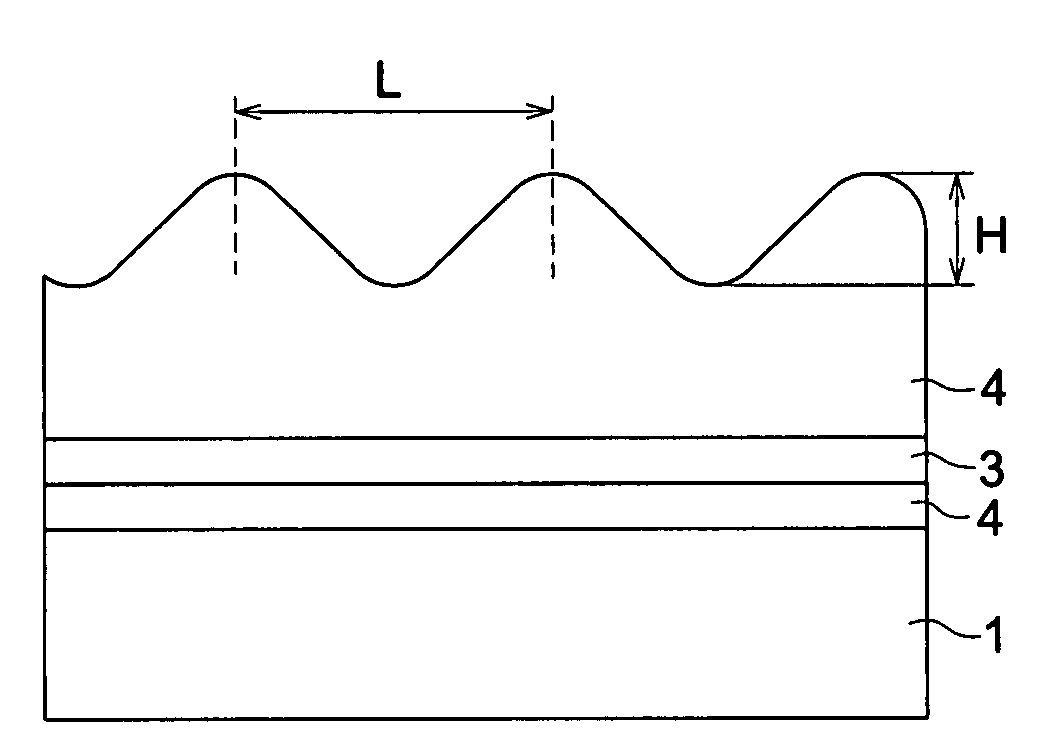
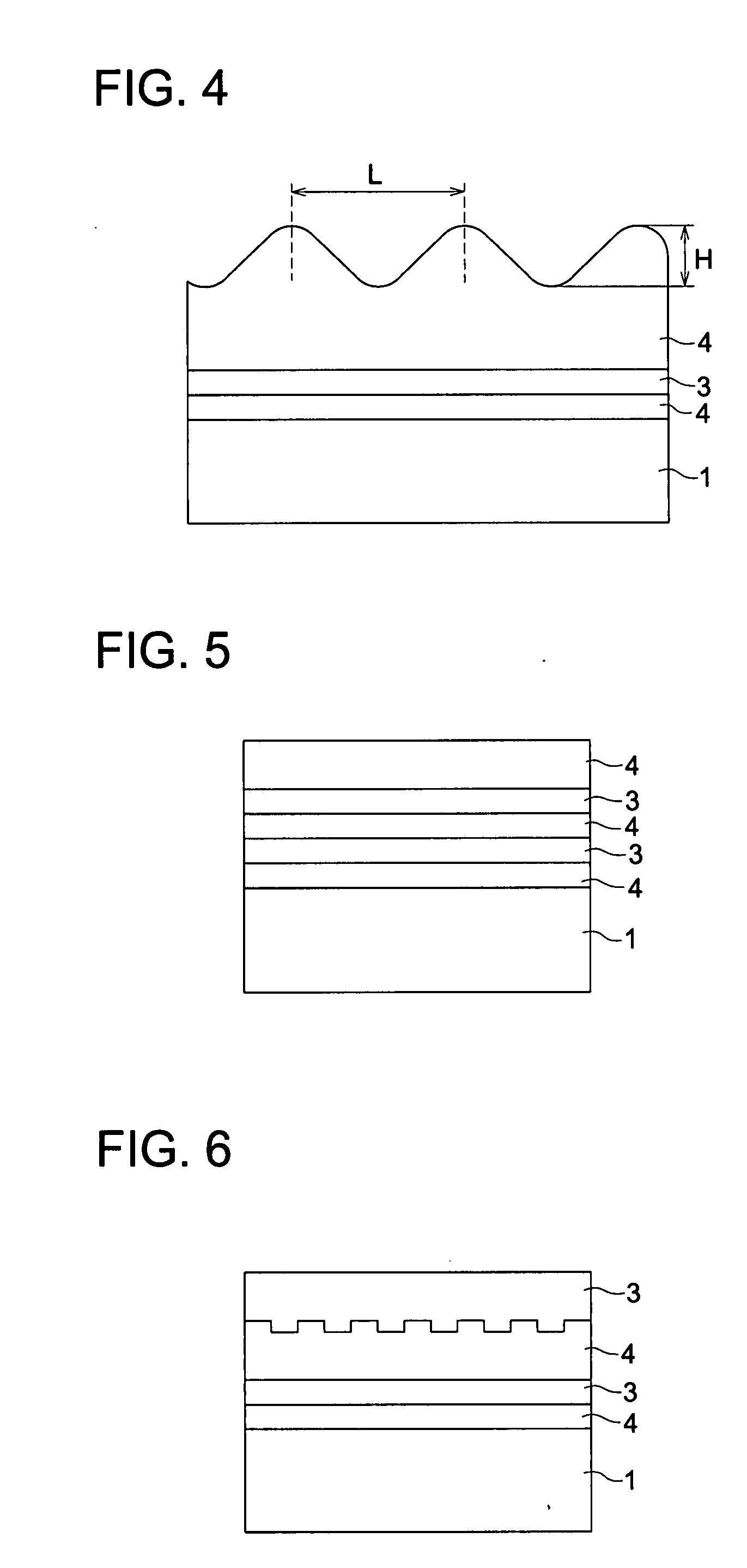
[0102]Next, the present invention is shown in FIG. 5.

[0103]This is an example of the resin film substrate which comprises a gas barrier layer which has a layer (diffusion layer) which diffracts or diffuses light which is also a stress relief layer on the outermost layer.

first embodiment

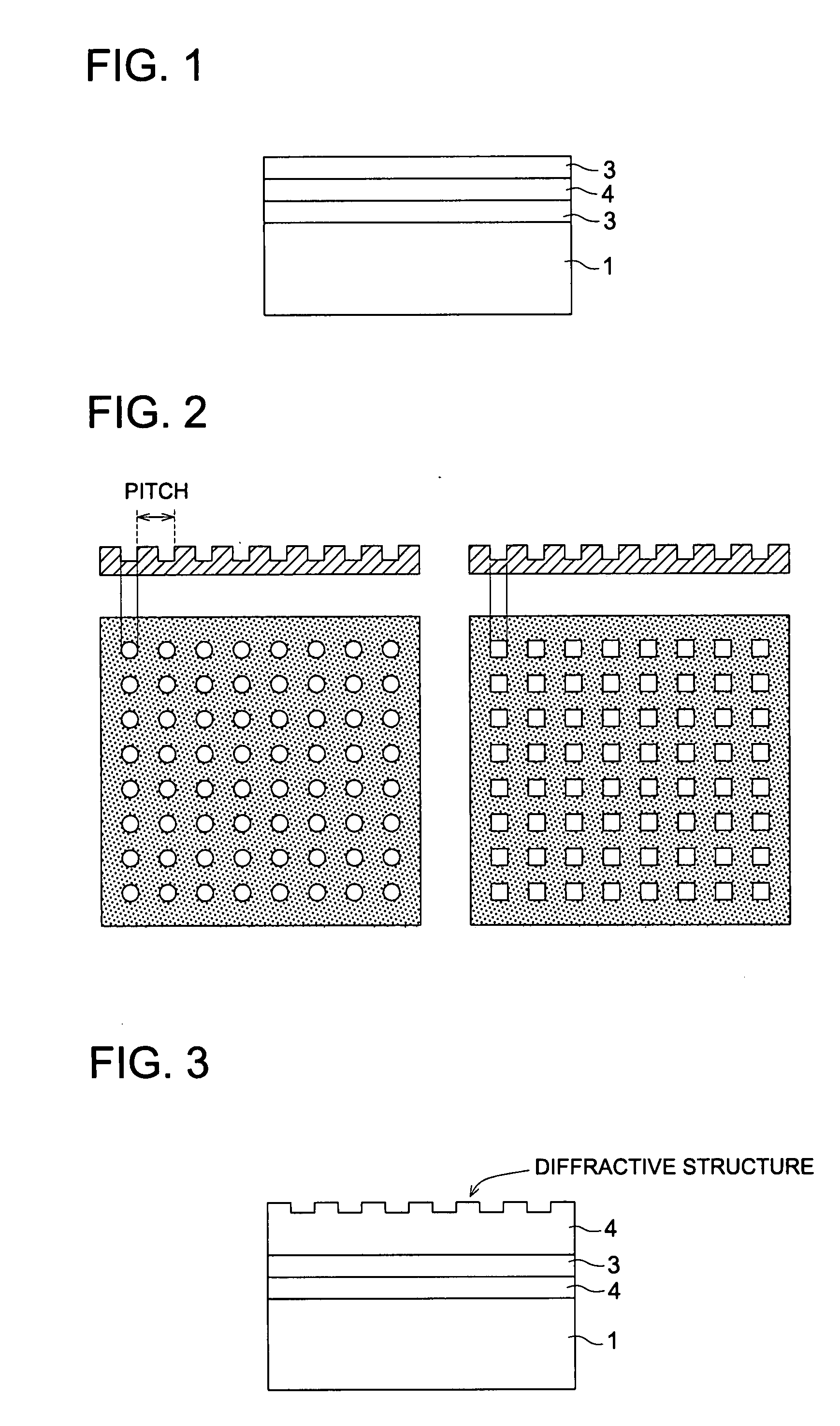
[0104]In the same manner as the first embodiment, the stress relief layer 4, as also an adhesive layer, is provided on a PES (thickness 200 μm) as a resin film substrate 1. That is to say, a vacuum deposition device is used and polymethyl methacrylate oligomer is introduced and deposited, and ultraviolet light is introduced in the same manner and polymerization is done to form a PMMA polymer film (thickness 200 μm). Next, in the same manner, on this film, a silicon oxide film is formed with a thickness of 200 μm by the plasma CVD method, and these are repeated and in the same manner, the PMMA layer (200 nm) which is the stress relief layer 4 as well as the gas barrier layer (silicon oxide layer) 3 which is 200 nm thick for example, is provided on the silicon oxide film.

[0105]In this embodiment, as a outermost layer, a diffusion layer (layer which diffracts or diffuses light) 5 which is also a stress relief layer is provided. Because this diffusion layer diffracts or diffuses light, ...

third embodiment

[0107]Next the present invention will be described.

[0108]In the first and second embodiment (FIGS. 3, 4 and 5), the layer having the concavo-convex structure for diffracting light provided on the outermost surface and the outermost layer (dispersion layer) which diffracts or diffuses light preferably have a refractive index which is as low as possible, and are also preferably (sufficiently) thicker (0.3 pm or more preferably 1 micron or more) than the wavelength. As a result, a portion of the light that will be totally reflected at the inside of the substrate can be taken out to the outside, and a substrate can be obtained in which the taking-out efficiency is further improved.

[0109]That is to say, the light that is totally reflected at the interface between the substrate and the outermost layer is reduced to an amount that is determined by the critical angle of the low refractive index layer. Thus the refractive index is preferably low and is preferably 1.50 or lower. The refractiv...


PUM

PropertyMeasurementUnit
Thicknessaaaaaaaaaa
Refractive indexaaaaaaaaaa

Abstract

Disclosed is a low-cost resin film substrate for organic electroluminescence which comprises a gas barrier layer having high gas barrier properties while being improved in light taking-out efficiency. Also disclosed is an organic electroluminescence device using such a resin film substrate. Specifically disclosed is a resin film substrate for organic electroluminescence comprising at least one gas barrier layer on a resin film. This resin Film substrate is characterized in that the surface of the outermost layer on the side having the gas barrier layer has a concavo-convex structure for diffracting of diffusing light.

Description

TECHNICAL FIELD[0001]The present invention relates to a resin film substrate for organic electroluminescence and an organic electroluminescence device using the organic film substrate.BACKGROUND ART[0002]In organic electroluminescence using a film substrate (also called organic EL hereinafter) light emitting device, there is a problem in that the light taking-out efficiency is low. Due to the effect of the refractive index of the light-emitting body, if the refractive index of the light emitting layer is, for example, 1.6-1.7, no more than about 20% of the total amount of emitted light can be taken out and most of the emitted light is totally reflected at the interface formed between the substrate and the light emitting layer for example and is trapped in the layer.[0003]A method of providing a structure for diffracting light at the total reflection interface has been proposed as a means for improving light taking-out efficiency (Patent Document 1).[0004]In addition, a method has be...

Claims


Application Information

Patent Timeline
IPC IPC(8): B32B3/00B32B9/04
CPCH01L51/0097H01L51/52H01L51/5237H01L51/5262H01L51/5268B32B27/08Y10T428/24612G02B5/0252G02B5/0278G02B5/0294G02B5/1866Y02E10/549Y10T428/24521G02B5/0231Y10T428/31504H10K77/111H10K50/80H10K50/8445H10K50/85H10K50/854H10K50/858H10K50/844H10K50/84
Inventor SATO, AKIRAHIRABAYASHI, SHIGETONAKAYAMA, TOMOYUKIKITA, HIROSHIFUKUDA, KAZUHIROTAKAHATA, TOSHIHIRO
Owner KONICA MINOLTA INC
Why Eureka
Try Eureka